SC1452 Просмотр технического описания (PDF) - Semtech Corporation
Номер в каталоге
Компоненты Описание
Список матч
SC1452 Datasheet PDF : 15 Pages
| |||
SC1452
POWER MANAGEMENT
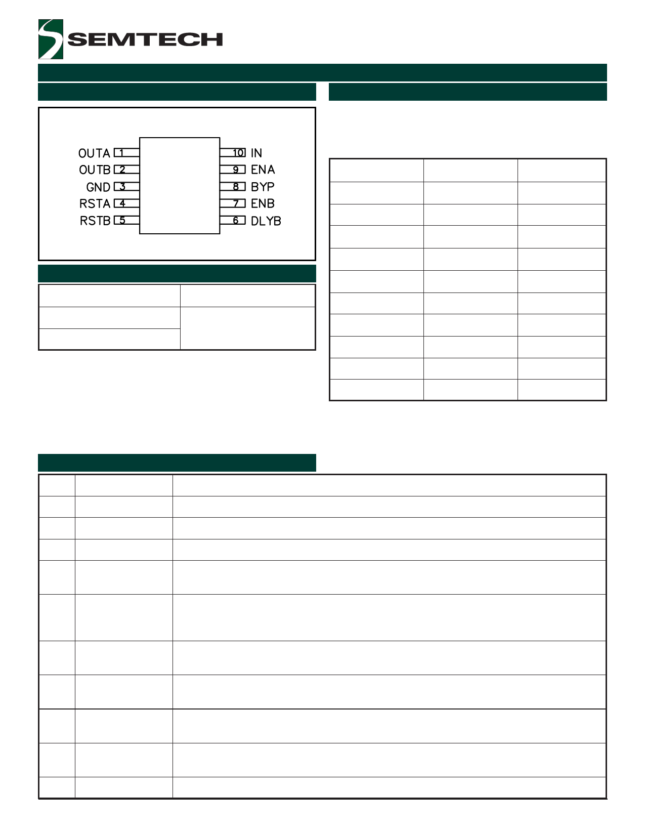
Pin Configuration
(Top View)
Voltage Options
Replace X in the part number (SC1452XIMS) by the
letter shown below for the corresponding voltage
option:
X
VOUTA (V)
VOUTB (V)
A
1.8
1.8
B
2.5
2.5
C
MSOP-10
D
Ordering Information
E
Part Numbers
Package
F
SC1452XIMSTR (1)(2)
MSOP-10
G
SC1452XIMSTRT (1)(2)(3)
H
Notes:
(1) Where X denotes voltage options - see Voltage
J
Options table.
K
(2) Only available in tape and reel packaging. A reel
contains 2500 devices.
(3) Lead-free product. This product is fully WEEE and
RoHS compliant.
2.8
2.8
3.0
3.0
3.3
3.3
3.0
2.5
3.0
1.8
3.0
2.8
3.3
2.5
3.3
2.8
Pin Descriptions
Pin #
Pin Name
Pin Function
1
OUTA
Regulator A output.
2
OUTB
Regulator B output.
3
GND
Ground pin.
4
RSTA
Power on reset for output A. Active low when OUTA is below the reset threshold. RSTA
goes high 50ms (typical) after OUTA rises above the reset threshold.
5
RSTB
Power on reset for output B. Active low when OUTB is below the reset threshold. RSTB
goes high 150ms (typical - can be adjusted using CDLYB) after OUTB rises above the reset
threshold.
6
DLYB
Programmable delay for RESETB. Delay time can be set by connecting a capacitor, CDLYB,
between this pin and ground. Ground this pin if using the default delay time.
7
ENB
Active high enable pin for output B. CMOS compatible input. Connect to IN if not being
used.
8
BYP
Bypass pin for bandgap reference. Connect a 10nF capacitor, CBYP, between this pin and
ground for low noise operation.
9
ENA
Active high enable pin for output A. CMOS compatible input. Connect to IN if not being
used.
10
IN
2006 Semtech Corp.
Input pin for both regulators.
5
www.semtech.com
Share Link: 