GLT6100L08LL-100TC Просмотр технического описания (PDF) - G-Link Technology
Номер в каталоге
Компоненты Описание
Список матч
GLT6100L08LL-100TC Datasheet PDF : 10 Pages
| |||
G-LINK
GLT6100L16
Ultra Low Power 64k x 16 CMOS SRAM
May 2000(Rev. 0.3)
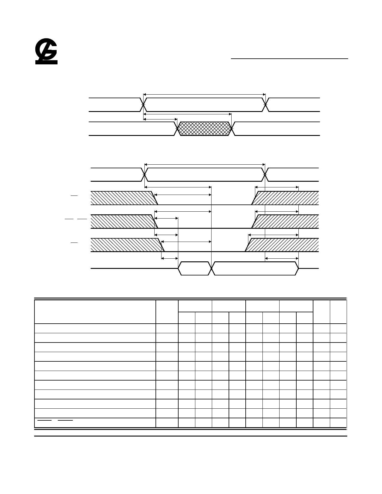
Timing Waveform of Read Cycle 1 (Address Controlled)
tRC
Address
tOH
tAA
DOUT
Previous Data Valid
Data Valid
Timing Waveform of Read Cycle 2 (14~16)
tRC
Address
tAA
tOH
CE
BLE / BHE
tBA
tLZ
tBLZ
tOE
OE
DOUT
High - Z
tOLZ
tHZ
tBHZ
tOHZ
tOH
Data Valid
Write Cycle (11)( Vcc=2.7V to 3.3V, TA = -25°C to + 85°C)
Parameter
Write Cycle Time
Chip Enable to Write End
Address Setup to Write End
Address Setup Time
Write Pulse Width
Write Recovery Time
Data Valid to Write End
Data Hold Time
Write Enable to Output in High-Z
Output Active from Write End
BLE , BHE Setup to Write End
G-Link Technology Corporation
2701 Northwestern Parkway
Santa Clara, CA 95051, U.S.A.
55
70
85
100
Symbol
Unit Note
Min Max Min Max Min Max Min Max
tWC
55
70
85
100
ns
tCW
50
60
70
80
ns
tAW
50
60
70
80
ns
tAS
0
0
0
0
ns
tWP
45
50
60
70
ns
tWR
0
0
0
0
ns
tDW
25
30
35
40
ns
tDH
0
0
0
0
ns
tWHZ
25
30
35
40 ns
tOW
5
5
5
5
ns
tBW
50
60
70
80
ns
-5-
G-Link Technology Corporation, Taiwan
6F No. 24-2, Industry E. RD. IV, Science Based
Industrial Park, Hsin Chu, Taiwan.
Share Link: 