RD74LVC1G79WPE Просмотр технического описания (PDF) - Renesas Electronics
Номер в каталоге
Компоненты Описание
Список матч
RD74LVC1G79WPE Datasheet PDF : 9 Pages
| |||
RD74LVC1G79
Single Positive Edge-triggered D-type Flip Flop
Description
REJ03D0695–0100
Rev.1.00
Feb 23, 2006
The RD74LVC1G79 has D-type flip flop in a 5-pin package. The input data is transferred to the output at the rising
edge of clock pulse CLK. Low voltage and high-speed operation is suitable for the battery powered products (e.g.,
notebook computers), and the low power consumption extends the battery life.
Features
• The basic gate function is lined up as Renesas uni logic series.
• Supply voltage range: 1.65 to 5.5 V
• Operating temperature range: –40 to +85°C
• All inputs: VIH (Max.) = 5.5 V (@VCC = 0 V to 5.5 V)
• All outputs: VO (Max.) = 5.5 V (@VCC = 0 V)
• Output current:
±4 mA (@VCC = 1.65 V)
±8 mA (@VCC = 2.3 V)
±24 mA (@VCC = 3.0 V)
±32 mA (@VCC = 4.5 V)
• Ordering Information
Part Name
Package Type
Package Code
(Previous Code)
RD74LVC1G79WPE
WCSP-5 pin
SXBG0005LB–A
(TBS-5CV)
Package
Abbreviation
WP
Taping Abbreviation
(Quantity)
E (3,000 pcs/reel)
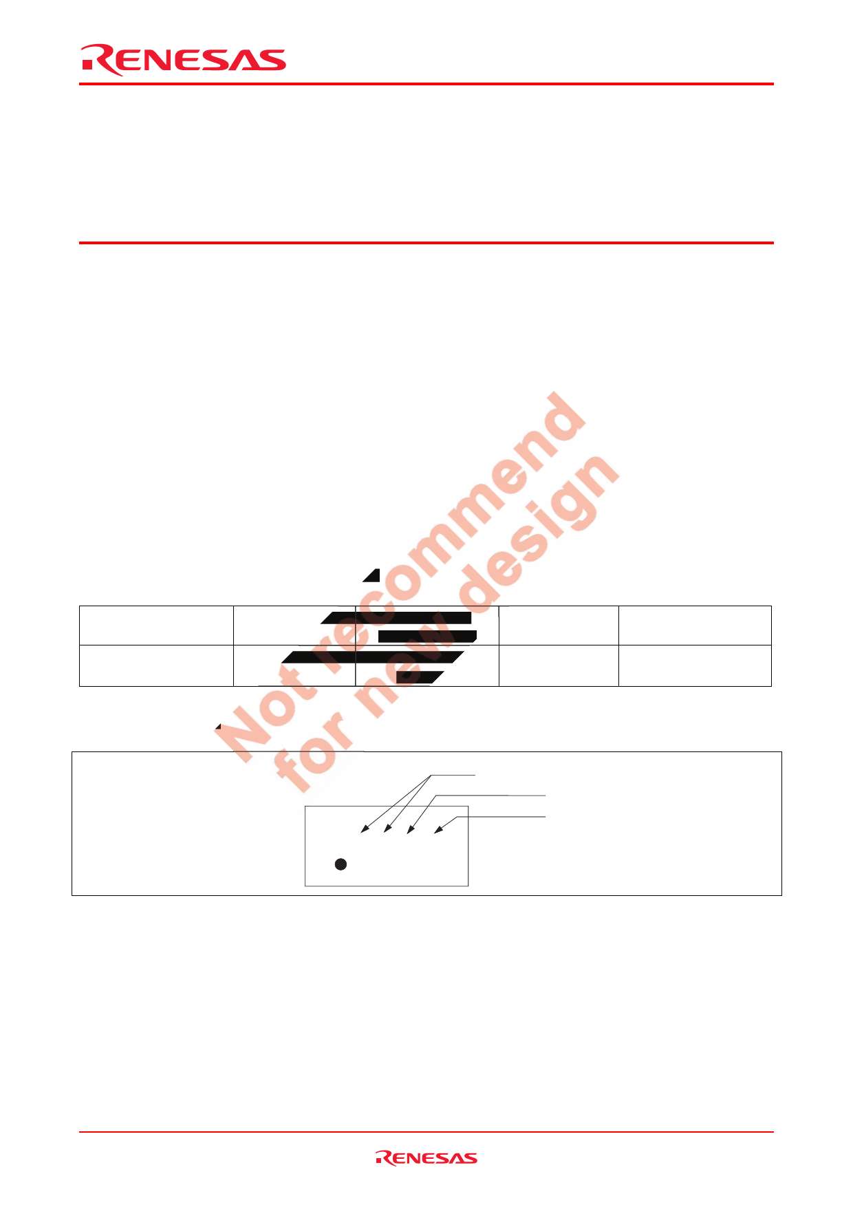
Article Indication
Marking
Year code
Month code
EF YM
Rev.1.00 Feb 23, 2006 page 1 of 6
Share Link: 