PCK2021DGG Просмотр технического описания (PDF) - Philips Electronics
Номер в каталоге
Компоненты Описание
Список матч
PCK2021DGG Datasheet PDF : 15 Pages
| |||
Philips Semiconductors
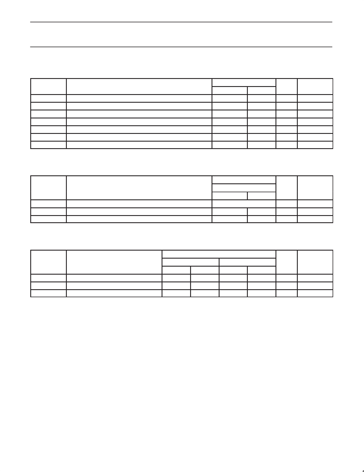
CK00 (100/133 MHz) spread spectrum differential
system clock generator
Product data
PCK2021
3V66 Outputs
Tamb = 0 to +70 °C
SYMBOL
PARAMETER
tPERIOD
tHIGH
tLOW
tRISE
tFALL
DUTY CYCLE
Period
High time
Low time
Rise time
Fall time
Duty cycle
tJITTER
Cycle-to-cycle jitter
REFER TO NOTES ON PAGE 10.
REF clock output
Tamb = 0 to +70 °C; lump capacitance test load = 20 pF
SYMBOL
PARAMETER
f
Frequency, actual
tJITTER
Cycle-to-cycle jitter
DUTY CYCLE Output duty cycle
REFER TO NOTES ON PAGE 10.
All outputs
Tamb = 0 to +70 °C
SYMBOL
PARAMETER
tPZL, tPZH
Output enable delay (all outputs)
tPZL, tPZH
Output disable delay (all outputs)
tSTABLE
All clock stabilization from power-up
REFER TO NOTES ON PAGE 10.
LIMITS
MIN
MAX
15.0
16.0
5.25
N/A
5.05
N/A
0.5
2.0
0.5
2.0
45
55
—
400
UNITS
ns
ns
ns
ns
ns
%
ps
NOTES
2, 3, 9, 19
5, 10, 19
6, 10, 19
8, 19
17, 19
17, 19
17, 19
LIMITS
48 MHz MODE
MIN
MAX
14.318
—
300
45
55
UNITS
MHz
ps
%
NOTES
16, 19
17, 19
17, 19
LIMITS
133 MHz MODE
100 MHz MODE
MIN
MAX
MIN
MAX
1.0
10.0
1.0
10.0
1.0
10.0
1.0
10.0
—
3
—
3
UNITS
ns
ns
ms
NOTES
19
19
7, 19
2001 Oct 11
9
Share Link: 