PCD5096 Просмотр технического описания (PDF) - Philips Electronics
Номер в каталоге
Компоненты Описание
Список матч
PCD5096 Datasheet PDF : 52 Pages
| |||
Philips Semiconductors
Universal codec
Preliminary specification
PCD5096
After reset, all the flip-flops are in a defined state, and the
IOM, DSP and codecs are in inactive mode. In typical
applications the universal codec is used with the
PCD5093, which provides a clock (GP_CLK7) and a reset
signal to the universal codec. The reset signal must be
generated by a microcontroller port bit. The RESET_OUT
pin of the PCD5093 cannot be used for this purpose,
because GP_CLK7 is stopped while RESET_OUT is LOW
after a Power-on-reset.
8 MEMORY AND CONTROL REGISTERS
8.1 DSP memories
The DSP in the PCD5096 has access to a 4k × 24-bit DSP
program ROM, a 512 × 16-bit XRAM and a 512 × 16-bit
YRAM.
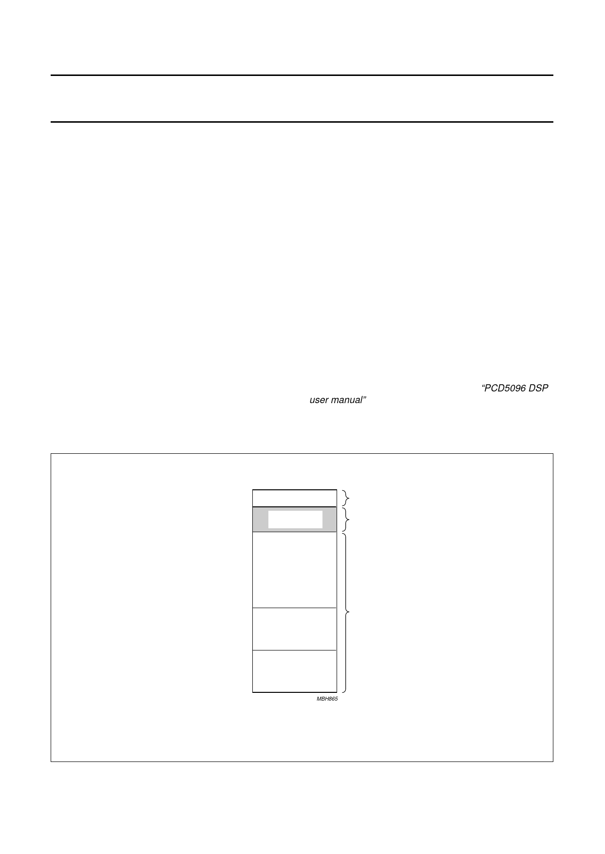
8.2 Data memory and control register map
The PCD5096 contains a 128 word (128 × 16-bit) System
Data RAM (SDR) and a group of 7 control registers
mapped onto the upper addresses of the SDR.
The registers and the SDR are byte and word accessible
externally, via the I2C-bus interface and internally via the
internal system bus.
The memory map is shown in Fig.6. The lower 32 words
contain the DSP parameter table. The next 32 words are
reserved for the IOM control table, which is used to control
the activity on the IOM-2 interface (maximum 32 slots per
8 kHz speech frame). The rest of the SDR addressable
space (40H to 77H) is free RAM and can be used to store
up to 14 IOM data buffer pairs. In cases where not all
14 IOM buffer pairs are needed this memory space can be
used for other applications via the I2C-bus. The same
holds for the unused part of the IOM control table.
The upper addresses of the SDR (78H to 7EH) are
mapped onto 7 control registers (CR0 to CR6) that control
the entire chip (DSP mode, data rate on the IOM-2
interface, control of the two codecs).
Note that the uppermost address of the SDR (7FH) is not
mapped to any hardware register and is addressable as a
normal RAM word.
The contents of the IOM control table and the IOM data
buffers are described in Chapter 9. For further details
about the DSP parameter table, see the “PCD5096 DSP
user manual”.
handbook, full pagewidth
1997 Jan 22
7FH
free RAM
7EH
control registers
78H
(7 words)
77H
SDR
hardware registers
IOM data buffers
and
free RAM
(14 x 4 words)
40H
3FH
IOM control table
(32 words)
20H
1FH
DSP parameter table
(32 words)
00H
MBH865
SDR
Fig.6 PCD5096 Memory map.
11
Share Link: 