PBL3853 Просмотр технического описания (PDF) - Ericsson
Номер в каталоге
Компоненты Описание
Список матч
PBL3853 Datasheet PDF : 16 Pages
| |||
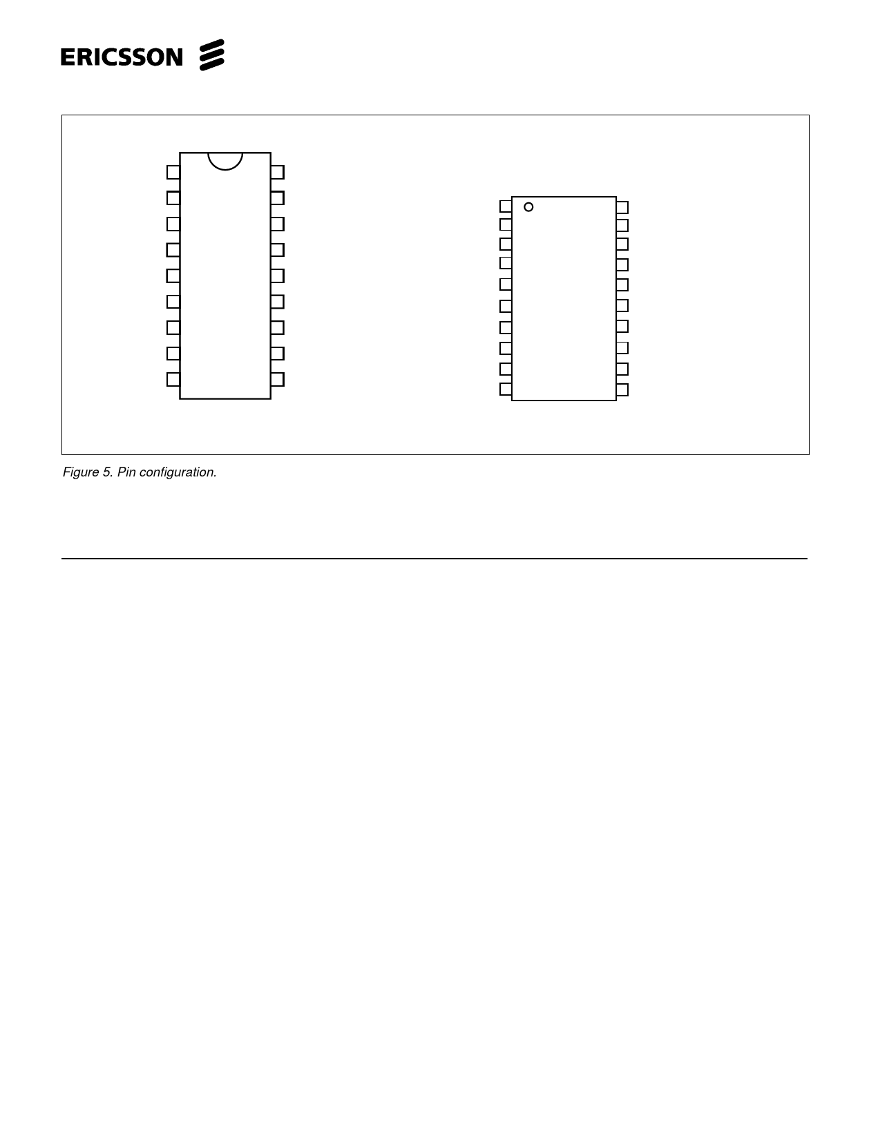
PBL 3853
+L 1
TO 2
TI 3
+C 4
DCAC 5
GR 6
T2 7
T1 8
FE 9
18 VDC
17 RI 2
16 RO
15 RI 1
14 -L
13 MI 2
12 MI 1
11 MO
10 TM
18 pin-DIP
+L 1
TO 2
TI 3
+C 4
DCAC 5
GR 6
T2 7
T1 8
FE 9
NC 10
20 pin-SO
20 VDC
19 RI2
18 RO
17 RI1
16 -L
15 MI 2
14 MI 1
13 MO
12 TM
11 NC
Figure 5. Pin configuration.
Pin Description
DIP SO
Symbol
1
1
+L
2
2
TO
3
3
TI
4
4
+C
5
5
DCAC
6
6
GR
7
7
T2
8
8
T1
9
9
FE
10 NC
11 NC
10 12 TM
11 13 MO
12 14 MI 1
13 15 MI 2
14 16 -L
15 17 RI1
16 18 RO
17 19 RI 2
18 20 VDC
Output of the transmitter (+Line side)
Output of the transmitter (side tone signal)
Input of the transmitter amplifier
The circuit supply (sinks ~ 0,3 mA)
Adjustment for DC-char. and AC imp. to line
Gain regulation starting point setting
Output for transistor 2, active when voltage on the line is too low for VDC
Output for transistor 1, active when charging current into VDC’s reservoir capacitor
Feedback
No connection
No connection
Transmitter mute input
Microphone amplifier output
Microphone amplifier inverting input
Microphone amplifier non inverting input
Negative terminal of the circuit
Receiver amplifier input (gain control)
Receiver amplifier output
Receiver amplifier input for cut-off, see page 7.
VDC supply terminal
5
Share Link: 