MC74HC4024D Просмотр технического описания (PDF) - Motorola => Freescale
Номер в каталоге
Компоненты Описание
Список матч
MC74HC4024D Datasheet PDF : 6 Pages
| |||
MC74HC4024
PIN DESCRIPTIONS
INPUTS
Clock (Pin 1)
Negative edge triggering clock input. A High to low transi-
tion of this input advances the state of the counter.
Reset (Pin 2)
Active high asynchronous reset. A high level applied to this
input resets the counter to its zero state, thus forcing all Q
outputs low.
OUTPUTS
Q1 – Q7 (Pins 12, 11, 9, 6, 5, 4, 3)
Active–high outputs. Each QN output divides the Clock in-
put frequency by 2N.
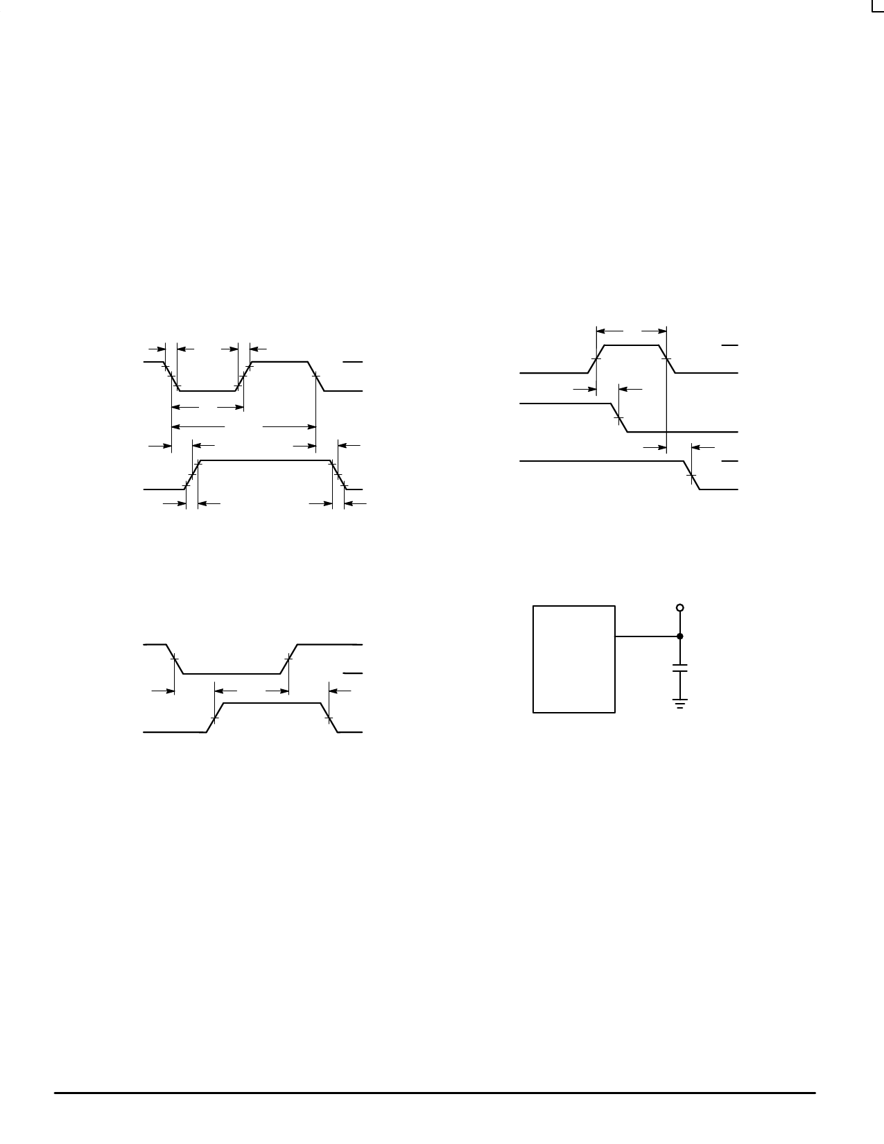
SWITCHING WAVEFORMS
tf
tr
90%
VCC
CLOCK
50%
10%
GND
tw
1/fmax
tPLH
tPHL
90%
Q1 50%
10%
tTLH
tTHL
Figure 1.
tw
VCC
RESET
50%
GND
tPHL
Q
CLOCK
50%
trec
VCC
50%
GND
Figure 2.
QN 50%
QN + 1
tPLH
50%
VCC
GND
tPHL
Figure 3.
TEST POINT
OUTPUT
DEVICE
UNDER
TEST
CL*
* Includes all probe and jig capacitance
Figure 4. Test Circuit
MOTOROLA
4
High–Speed CMOS Logic Data
DL129 — Rev 6
Share Link: 