AD9802 Просмотр технического описания (PDF) - Analog Devices
Номер в каталоге
Компоненты Описание
Список матч
AD9802 Datasheet PDF : 20 Pages
| |||
AD9802
APPLICATIONS INFORMATION
Generating Clock Signals
1V p-p
CIN
ADCIN
For best performance, the AD9802 should be driven by 3 V
logic levels. As shown in the Equivalent Input Circuits, the use
RBIAS
CML
SHA
of 5 V logic for ADCCLK will turn on the protection diode to
DVDD, increasing the current flow into this pin. As a result,
RBIAS SHABYP
noise and power dissipation will increase. The CDS clock in-
1.5V
puts, SHP and SHD, have a additional protection and can with-
stand direct 5 V levels.
AD9802
+3V
ADCMODE
External clamping diodes or resistor dividers can be used to
translate 5 V levels to 3 V levels, but the lowest power dissi-
pation is achieved with a logic transceiver chip. National
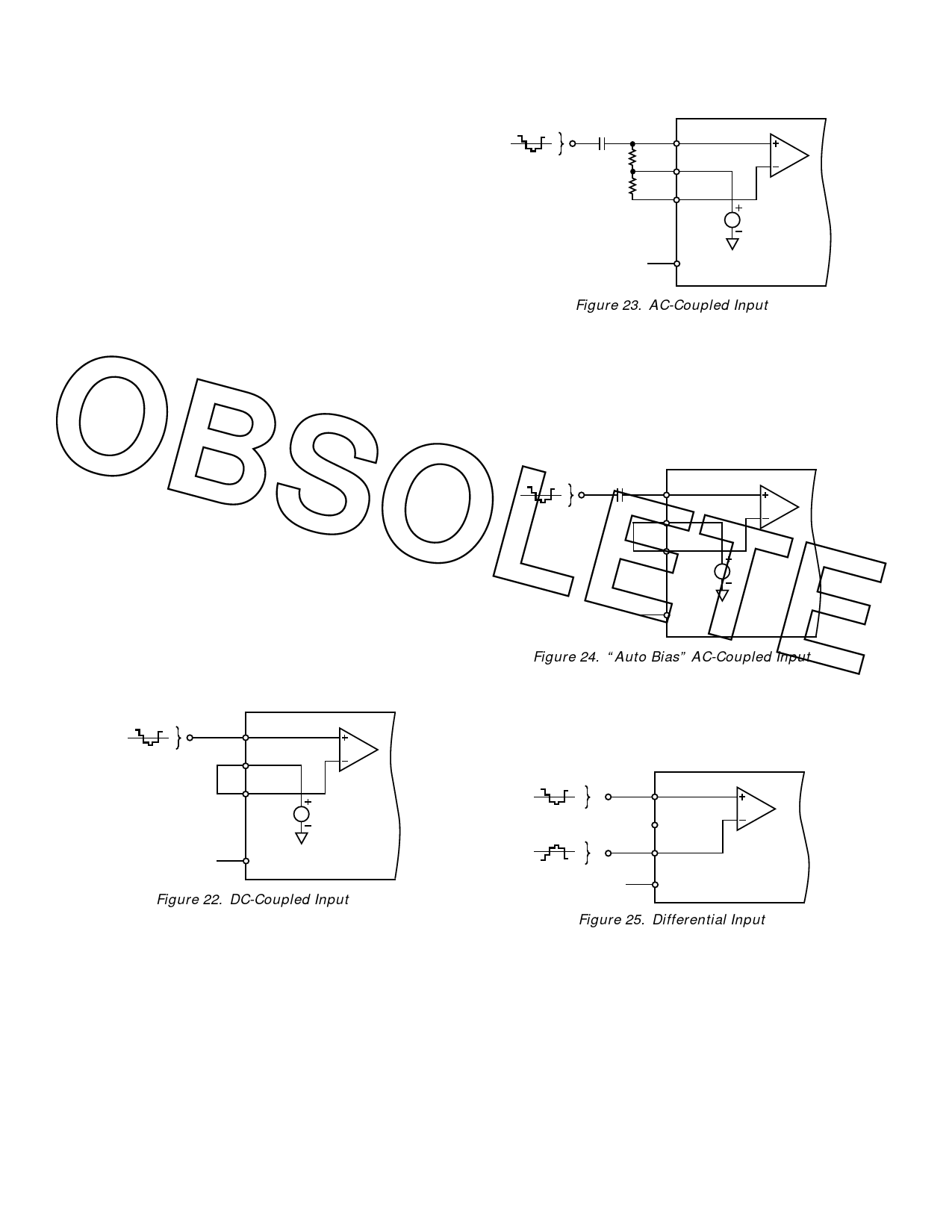
Figure 23. AC-Coupled Input
Semiconductor’s 74LVX4245 provides a 5 V to 3 V level shift
Figure 24 shows an alternative ac-coupled configuration. By
OBSOLETE for up to eight clock signals, has a three-state option, and
features low power consumption. Philips Semiconductor and
Quality also manufacture similar devices.
Driving the Direct ADC Input
The AD9802 can be used in a “direct ADC input” mode, in
which the input signal bypasses the input clamp, CDS and
PGA, and is sent directly to the sample and hold amplifier (SHA)
of the ADC. There are several methods that may be used to
drive the direct ADC input.
To enable the direct input mode of operation, ADCMODE (Pin
41) is taken to logic high. This will internally disconnect the
PGA output from the SHA input, and connect ADCIN (Pin 36)
to the SHA input.
The SHA has a differential input, consisting of ADCIN (Pin 36)
as the positive input, and SHABYP (Pin 38) as the negative
input. Both pins must be properly dc biased.
connecting SHABYP to CML, the dc bias at Pin 36 (ADCIN)
will internally track to the same voltage, automatically setting
the input bias level. With a given input capacitor value, CIN, the
time constant in this configuration will be dependent on the
sampling frequency FS. Specifically:
τ = (CIN/FS) × 2E +12
1V p-p
CIN
+3V
ADCIN
CML
SHA
SHABYP
1.5V
ADCMODE
AD9802
Figures 22 through 25 show four circuits for driving the direct
ADC input. Decoupling capacitors are not shown for CML,
Figure 24. “Auto Bias” AC-Coupled Input
VRT, VRB and SHABYP pins.
Figure 25 shows a true differential drive circuit. Each input
would be 500 mV p-p, to achieve the 1 V full-scale input to the
1V p-p
CML
ADCIN
CML
SHA
ADC. The common-mode input range for this configuration
extends from about 500 mV to 2.5 V. This circuit could also be
implemented with ac coupling, similar to Figure 23.
SHABYP
500mV p-p
ADCIN
1.5V
AD9802
+3V
ADCMODE
Figure 22. DC-Coupled Input
Figure 22 is a single-ended, dc-coupled circuit. SHABYP is
connected to CML (1.5 V) to establish a midpoint bias. The
input signal of 1 V p-p should be centered around CML.
Figure 23 shows an ac-coupled configuration, where both inputs
are biased to CML. The input capacitor CIN and bias resistors
should be sized to set the appropriate high pass cutoff frequency
for the application. To minimize the differential offset voltage
due to the input bias currents, both resistors should be equal.
500mV p-p
+3V
CML
SHABYP
ADCMODE
SHA
AD9802
Figure 25. Differential Input
Figure 26 shows a video clamp circuit which may be used with
the direct ADC mode of the AD9802 (supplies and decoupling
not shown). The circuit will clamp the reference black level of
an incoming video signal to 1.25 V dc. With SHABYP con-
nected to 1.75 V (VRT), the ADCIN range spans from 1.25 V
to 2.25 V. To accomplish this, the CLAMP pulse should be
asserted during the horizontal sync interval, when the video is at
its reference black level. A 5 V logic high applied to the gate of
the SD210 will turn on the device, and the input capacitor CIN
will charge up to provide 1.25 V at the ADCIN pin of the
AD9802. Other appropriate NMOS devices may be substituted
for the SD210. The AD8047 op amp requires ± 5 V supplies;
appropriate single supply op amps may be substituted. The size
of capacitor CIN should be set to meet the acquisition time and
–10–
REV. 0
Share Link: 