MX93002 Просмотр технического описания (PDF) - Macronix International
Номер в каталоге
Компоненты Описание
Список матч
MX93002 Datasheet PDF : 35 Pages
| |||
MX93002
SPK-DRV turns on
( ALC1 , ALC0 ) D(7,1) = (0,0) : ALC open loop gain is 38dB
= (0,1) : ALC open loop gain is 42dB
= (1,0) : reserved
= (1,1) : external ALC option ( PRE-PGA Output : ALCC1, SWC path “ a” Input : ALCC2)
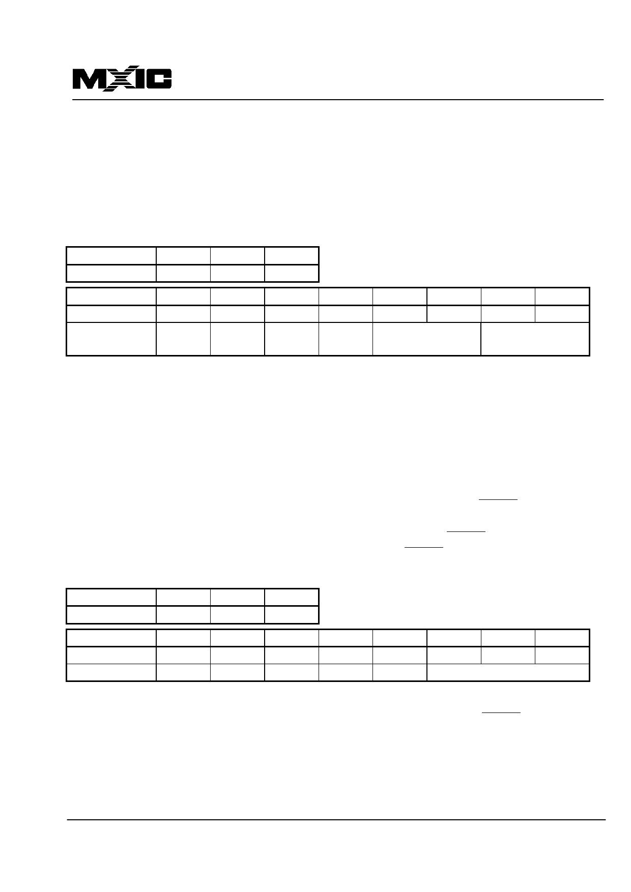
REGISTER 6
ADDRESS BIT
A2
A1
A0
DATA
1
1
0
DATA BIT
D7
D6
D5
D4
D3
D2
D1
D0
POWER_ON
0
0
0
0
0
0
0
0
DESCRIPTION SLEEPA SLEEP SWL
SPK-
SPK-DRV GAIN
AD1-PGA GAIN
MUTE
SETTING
SETTING
( SLEEPA , SLEEP ) D(7,6) = (0,0) : when the MX93002 gets into power down mode, all the blocks of the MX93002
will be disabled except the VBG reference and 2 comparators (POW, BAT)
D(7,6) = (0,1) : when the MX93002 gets into power down mode, all the blocks of the MX93002
will be disabled
D(7,6) = (1,0) : when the MX93002 gets into power down mode, all the blocks of the MX93002
will be disabled except 2 comparators (POW, BAT)
D(7,6) = (1,1) : when the MX93002 gets into power down mode, all the analog blocks of the
MX93002 will be still functional and can be programmed by control registers
( SWL ) D(5) = (1) : path of SWL is "CLOSE", D(5) = (0) : path of SWL is "OPEN” ; see NOTE 7
( SPK-MUTE ) D(4) = 1 : force SPK-DRV mute to -70dB, D(4) = 0 : force SPK-DRV un-mute
( SPK-DRV GAIN SETTING ) D(3,2) = (0,0) ~ (1,1) : 0dB ~ 8dB; 2dB/step; see NOTE 5
( AD1-PGA GAIN SETTING ) D(1,0) = (0,0) ~ (1,1) : 0dB ~ 18dB; see NOTE 2
REGISTER 7
ADDRESS BIT A2
A1
A0
DATA
1
1
1
DATA BIT
D7
D6
D5
D4
D3
D2
D1
D0
POWER_ON
0
0
0
0
0
0
0
0
DESCRIPTIN
SWO
SWN
READ
REGISTER ADDRESS
( SWO ) D(5) = (1) : path of SWO is "CLOSE", D(5) = (0) : path of SWO is "OPEN”
( SWN ) D(4) = (1) : path of SWN is "CLOSE", D(5) = (0) : path of SWN is "OPEN” ; see NOTE 7
( READ ) D(3) = 1 : read data from Register 0 ~ 7, D(3) = 0 : write data to Register 0 ~ 7
( REGISTER ADDRESS ) D(2~0) : When READ = 1, then
a. READ will be cleared automatically;
b. if next uP SDENB signal active low, the content of REGISTER ADDRESS will be dumped out through
CODEC SDATA interface;
14
Share Link: 