MT88E45B Просмотр технического описания (PDF) - Zarlink Semiconductor Inc
Номер в каталоге
Компоненты Описание
Список матч
MT88E45B Datasheet PDF : 28 Pages
| |||
Data Sheet
MT88E45B
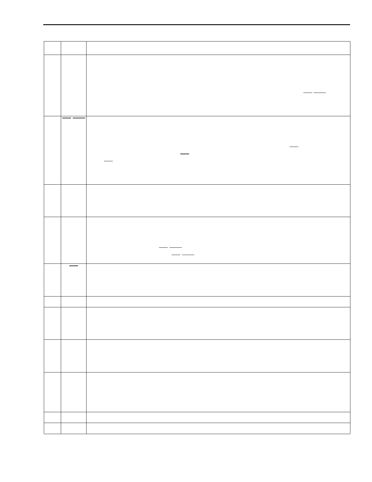
Pin Description
Pin # Name
Description
10 DATA 3-wire FSK Interface Data (CMOS Output). Mark frequency corresponds to logical 1. Space
frequency corresponds to logical 0.
In mode 0 (when the CB0 pin is logic low) the FSK serial bit stream is output to the DATA pin
directly.
In mode 1 (when the CB0 pin is logic high) the start bit is stripped off, the data byte and the trailing
stop bit are stored in a 9 bit buffer. At the end of each word signalled by the DR/STD pin, the
microcontroller should shift the byte out onto the DATA pin by applying 8 read pulses to the DCLK
pin. A 9th DCLK pulse will shift out the stop bit for framing error checking.
11 DR/STD 3-wire FSK Interface Data Ready/CAS Detection Delayed Steering (CMOS Output). Active
low.
When FSK demodulation is enabled via the CB1 and CB2 pins this pin is the Data Ready output.
It denotes the end of a word. In both FSK interface modes 0 and 1, it is normally hi and goes low
for half a bit time at the end of a word. But in mode 1 if DCLK starts during DR low, the first rising
edge of the DCLK input will return DR to high. This feature allows an interrupt requested by a low
going DR to be cleared upon reading the first DATA bit.
When CAS detection is enabled via the CB1 and CB2 pins this pin is the Delayed Steering output.
It goes low to indicate that a time qualified CAS has been detected.
12 EST CAS Detection Early Steering (CMOS Output). Active high. This pin is the raw CAS detection
output. It goes high to indicate the presence of a signal meeting the CAS accept frequencies and
signal level. It is used in conjunction with the ST/GT pin and external components to time qualify
the detection to determine whether the signal is a real CAS.
13 ST/GT CAS Detection Steering/Guard Time (CMOS Output/Analog Input). It is used in conjunction
with the EST pin and external components to time qualify the detection to determine whether the
signal is a real CAS.
A voltage greater than VTGt at this pin causes the MT88E45B to indicate that a CAS has been
detected by asserting the DR/STD pin low. A voltage less than VTGt frees up the MT88E45B to
accept a new CAS and returns DR/STD to high.
14 CD Carrier Detect (CMOS Output). Active low.
A logic low indicates that an FSK signal is present. A time hysteresis is provided to allow for
momentary signal discontinuity. The demodulated FSK data is ignored by the MT88E45B until
carrier detect has been activated.
15 Vdd Positive power supply.
16 CB1 Control Bit 1 (CMOS Input). Together with CB2 this pin selects the MT88E45B’s functionality
between FSK demodulation, Tip/Ring CAS detection and Hybrid CAS detection.
When CB0 is high and CB1, CB2 are both low the MT88E45B is put into a power down state
consuming minimal power supply current. See Tables 1 and 2.
17 CB2 Control Bit 2 (CMOS Input). Together with CB1 this pin selects the MT88E45B’s functionality
between FSK demodulation, Tip/Ring CAS detection and Hybrid CAS detection.
When CB0 is high and CB1, CB2 are both low the MT88E45B is put into a power down state
consuming minimal power supply current. See Tables 1 and 2.
18 GS2 Hybrid Gain Select (Output). This is the output of the hybrid receive connection op-amp. The op-
amp should be used to connect the MT88E45B to the telephone hybrid or speech IC receive pair.
The hybrid receive signal can be amplified or attenuated at GS2 via selection of the feedback
resistor between GS2 and IN2-. When the CPE is off-hook CAS detection of the GS2 signal
should be enabled via the CB1 and CB2 pins. See Tables 1 and 2.
19 IN2- Hybrid Op-amp Inverting (Input).
20 IN2+ Hybrid Op-amp Non-Inverting (Input).
3
Share Link: 