MCM6709RJ6 Просмотр технического описания (PDF) - Motorola => Freescale
Номер в каталоге
Компоненты Описание
Список матч
MCM6709RJ6 Datasheet PDF : 8 Pages
| |||
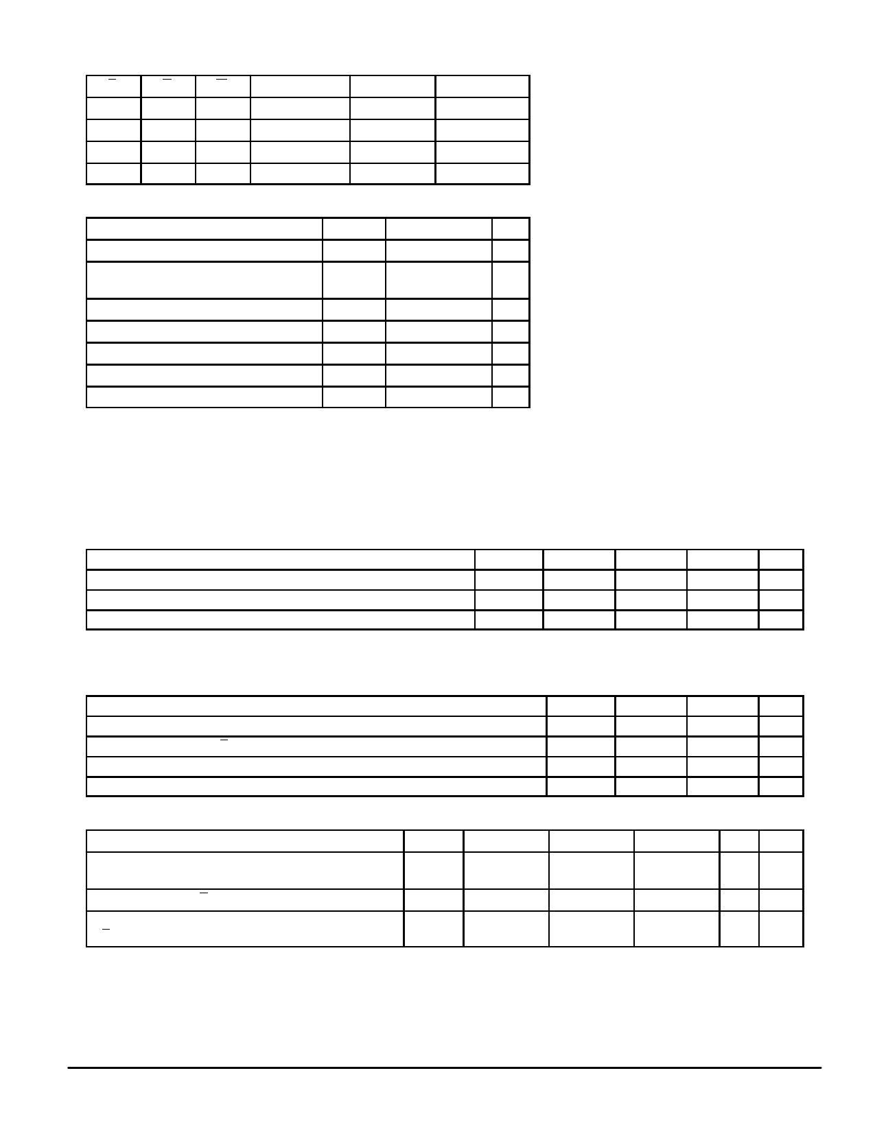
TRUTH TABLE (X = Don’t Care)
E
G
W
Mode
H
X
X
Not Selected
L
H
H
Read
L
L
H
Read
L
X
L
Write
Output
High–Z
High–Z
Dout
Din
Cycle
—
—
Read Cycle
Write Cycle
ABSOLUTE MAXIMUM RATINGS (See Note)
Rating
Symbol
Value
Unit
Power Supply Voltage
VCC
– 0.5 to + 7.0
V
Voltage Relative to VSS for Any Pin
Except VCC
Vin, Vout – 0.5 to VCC + 0.5 V
Output Current (per I/O)
Iout
± 30
mA
Power Dissipation
PD
2.0
W
Temperature Under Bias
Tbias
– 10 to + 85
°C
Operating Temperature
TA
0 to + 70
°C
Storage Temperature — Plastic
Tstg
– 55 to + 125
°C
NOTE: Permanent device damage may occur if ABSOLUTE MAXIMUM RATINGS are
exceeded. Functional operation should be restricted to RECOMMENDED OPER-
ATING CONDITIONS. Exposure to higher than recommended voltages for
extended periods of time could affect device reliability.
This device contains circuitry to protect the
inputs against damage due to high static volt-
ages or electric fields; however, it is advised
that normal precautions be taken to avoid appli-
cation of any voltage higher than maximum
rated voltages to this high–impedance circuit.
This BiCMOS memory circuit has been de-
signed to meet the dc and ac specifications
shown in the tables, after thermal equilibrium
has been established. The circuit is in a test
socket or mounted on a printed circuit board
and transverse air flow of at least 500 linear feet
per minute is maintained.
DC OPERATING CONDITIONS AND CHARACTERISTICS
(VCC = 5.0 V ± 10%, TA = 0 to 70°C, Unless Otherwise Noted)
RECOMMENDED OPERATING CONDITIONS
Parameter
Symbol
Min
Supply Voltage (Operating Voltage Range)
Input High Voltage
VCC
4.5
VIH
2.2
Input Low Voltage
VIL
– 0.5**
* VIH (max) = VCC + 0.3 V dc; VIH (max) = VCC + 2.0 V ac (pulse width ≤ 2.0 ns) or I ≤ 30.0 mA.
** VIL (min) = – 0.5 V dc @ 30.0 mA; VIL (min) = – 2.0 V ac (pulse width ≤ 2.0 ns) or I ≤ 30.0 mA.
Typ
Max
Unit
5.0
5.5
V
—
VCC + 0.3* V
—
0.8
V
DC CHARACTERISTICS
Parameter
Input Leakage Current (All Inputs, Vin = 0 to VCC)
Output Leakage Current (E = VIH, Vout = 0 to VCC)
Output High Voltage (IOH = – 4.0 mA)
Output Low Voltage (IOL = 8.0 mA)
Symbol
Min
Ilkg(I)
—
Ilkg(O)
—
VOH
2.4
VOL
—
Max
Unit
± 1.0
µA
± 1.0
µA
—
V
0.4
V
POWER SUPPLY CURRENTS
Parameter
Symbol MCM6709R–6 MCM6709R–7 MCM6709R–8 Unit
AC Active Supply Current (Iout = 0 mA,
VCC = max, f = fmax)
ICCA
195
190
185
mA
AC Standby Current (E = VIH, VCC = max, f = fmax)
ISB1
85
80
75
mA
CMOS Standby Current (VCC = max, f = 0 MHz,
E ≥ VCC – 0.2 V, Vin ≤ VSS, or ≥ VCC – 0.2 V)
ISB2
20
20
20
mA
NOTES:
1. Reference AC Operating Conditions and Characteristics for input and timing (VIH/VIL, tr/tf, pulse level 0 to 3 V, VIH = 3 V).
2. All addresses transition simultaneously low (LSB) and then high (MSB).
3. Data states are all zero.
Notes
1, 2, 3
1, 2, 3
MCM6709R
2
MOTOROLA FAST SRAM
Share Link: 