MC74LCX02D Просмотр технического описания (PDF) - ON Semiconductor
Номер в каталоге
Компоненты Описание
Список матч
MC74LCX02D Datasheet PDF : 8 Pages
| |||
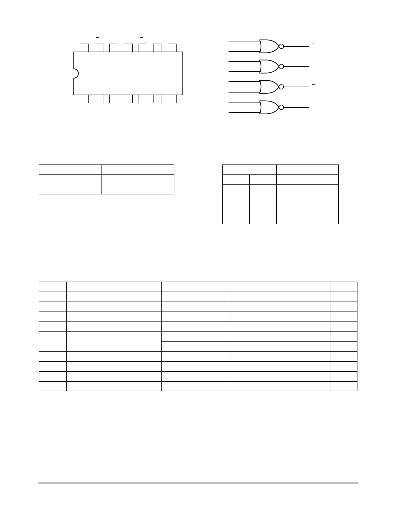
MC74LCX02
VCC O2 B2 A2 O3 B3 A3
14 13 12 11 10 9 8
1234567
O0 A0 B0 O1 A1 B1 GND
Figure 1. Pinout: 14−Lead (Top View)
A0 2
3
B0
A1 5
6
B1
11
A2
B2 12
8
A3
B3 9
1
O0
4
O1
13
O2
10
O3
Figure 2. Logic Diagram
PIN NAMES
Pins
An, Bn
On
Function
Data Inputs
Outputs
TRUTH TABLE
Inputs
An
Bn
L
L
L
H
H
L
H
H
Outputs
On
H
L
L
L
H = High Voltage Level
L = Low Voltage Level
For ICC reasons, DO NOT FLOAT Inputs
MAXIMUM RATINGS
Symbol
Parameter
Value
Condition
Unit
VCC
DC Supply Voltage
−0.5 to +7.0
V
VI
DC Input Voltage
−0.5 ≤ VI ≤ +7.0
V
VO
DC Output Voltage
−0.5 ≤ VO ≤ VCC + 0.5
Output in HIGH or LOW State (Note 1)
V
IIK
DC Input Diode Current
−50
VI < GND
mA
IOK
DC Output Diode Current
−50
VO < GND
mA
+50
VO > VCC
mA
IO
DC Output Source/Sink Current
±50
mA
ICC
DC Supply Current Per Supply Pin
±100
mA
IGND
DC Ground Current Per Ground Pin
±100
mA
TSTG
Storage Temperature Range
−65 to +150
°C
Maximum ratings are those values beyond which device damage can occur. Maximum ratings applied to the device are individual stress limit
values (not normal operating conditions) and are not valid simultaneously. If these limits are exceeded, device functional operation is not implied,
damage may occur and reliability may be affected.
1. IO absolute maximum rating must be observed.
http://onsemi.com
2
Share Link: 