MC74LCX02D Просмотр технического описания (PDF) - ON Semiconductor
Номер в каталоге
Компоненты Описание
Список матч
MC74LCX02D Datasheet PDF : 8 Pages
| |||
MC74LCX02
Low−Voltage CMOS Quad
2−Input NOR Gate
With 5 V−Tolerant Inputs
The MC74LCX02 is a high performance, quad 2−input NOR gate
operating from a 2.3 to 3.6 V supply. High impedance TTL compatible
inputs significantly reduce current loading to input drivers while TTL
compatible outputs offer improved switching noise performance. A VI
specification of 5.5 V allows MC74LCX02 inputs to be safely driven
from 5 V devices.
Current drive capability is 24 mA at the outputs.
Features
• Designed for 2.3 V to 3.6 V VCC Operation
• 5 V Tolerant Inputs − Interface Capability With 5 V TTL Logic
• LVTTL Compatible
• LVCMOS Compatible
• 24 mA Balanced Output Sink and Source Capability
• Near Zero Static Supply Current (10 mA) Substantially Reduces
System Power Requirements
• Latchup Performance Exceeds 500 mA
• ESD Performance: Human Body Model >2000 V;
Machine Model >200 V
• Pb−Free Packages are Available*
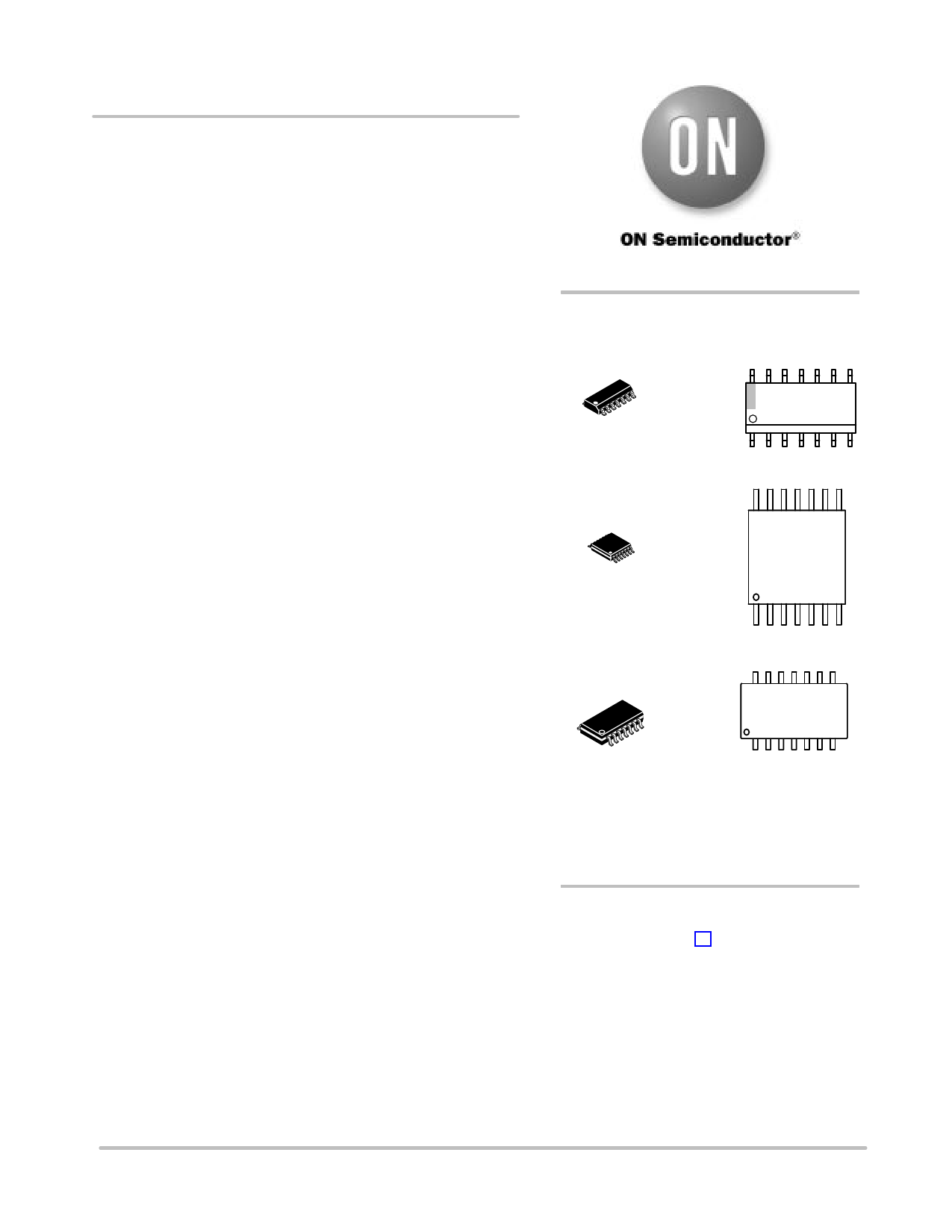
14
1
http://onsemi.com
MARKING
DIAGRAMS
14
SOIC−14
D SUFFIX
CASE 751A
1
LCX02
AWLYWW
14
14
1
TSSOP−14
DT SUFFIX
CASE 948G
LCX
02
ALYW
14
1
1
14
SOEIAJ−14
M SUFFIX
CASE 965
74LCX02
ALYW
1
A
= Assembly Location
L, WL = Wafer Lot
Y
= Year
W, WW = Work Week
ORDERING INFORMATION
See detailed ordering and shipping information in the package
dimensions section on page 4 of this data sheet.
*For additional information on our Pb−Free strategy and soldering details, please
download the ON Semiconductor Soldering and Mounting Techniques
Reference Manual, SOLDERRM/D.
© Semiconductor Components Industries, LLC, 2005
1
January, 2005 − Rev. 5
Publication Order Number:
MC74LCX02/D
Share Link: 