MB3778 Просмотр технического описания (PDF) - Fujitsu
Номер в каталоге
Компоненты Описание
Список матч
MB3778 Datasheet PDF : 31 Pages
| |||
MB3778
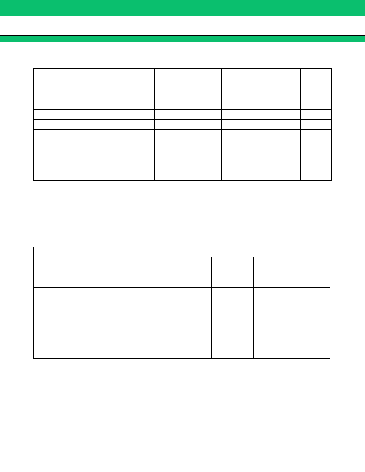
■ ABSOLUTE MAXIMUM RATINGS
Parameter
Symbol
Condition
Rating
Unit
Min
Max
Power Supply Voltage
VCC
⎯
⎯
20
V
Error Amp Input Voltage
VIN
⎯
−0.3
+10
V
Control Input Voltage
VCTL
⎯
−0.3
+20
V
Collector Output Voltage
VOUT
⎯
⎯
20
V
Collector Output Current
IOUT
⎯
⎯
75
mA
Power Dissipation
Ta ≤ +25 °C (SOP)
⎯
PD
Ta ≤ +25 °C (SSOP)
⎯
620*1
mW
444*2
mW
Operating Ambient Temperature Ta
⎯
−30
+85
°C
Storage Temperature
Tstg
⎯
−55
+125
°C
*1: The packages are mounted on the epoxy board (4 cm × 4 cm)
*2: The packages are mounted on the epoxy board (10 cm × 10 cm)
WARNING: Semiconductor devices can be permanently damaged by application of stress (voltage, current,
temperature, etc.) in excess of absolute maximum ratings. Do not exceed these ratings.
■ RECOMMENDED OPERATING CONDITIONS
Parameter
Symbol
Min
Value
Typ
Unit
Max
Power Supply Voltage
Error Amp Input Voltage
Control Input Voltage
Collector Output Voltage
Collector Output Current
Timing Capacitor
Timing Resistor
Oscillator Frequency
Operating Ambient Temperature
VCC
VIN
VCTL
VOUT
IOUT
CT
RT
fOSC
Ta
3.6
1.05
0
⎯
0.3
150
5.1
1
−30
6.0
18
V
⎯
1.45
V
⎯
18
V
⎯
18
V
⎯
50
mA
⎯
15000
pF
⎯
100
kΩ
⎯
500
kHz
+25
+85
°C
WARNING: The recommended operating conditions are required in order to ensure the normal operation of the
semiconductor device. All of the device’s electrical characteristics are warranted when the device is
operated within these ranges.
Always use semiconductor devices within their recommended operating condition ranges. Operation
outside these ranges may adversely affect reliability and could result in device failure.
No warranty is made with respect to uses, operating conditions, or combinations not represented on
the data sheet. Users considering application outside the listed conditions are advised to contact their
FUJITSU representatives beforehand.
6
Share Link: 