MB3778 Просмотр технического описания (PDF) - Fujitsu
Номер в каталоге
Компоненты Описание
Список матч
MB3778 Datasheet PDF : 31 Pages
| |||
MB3778
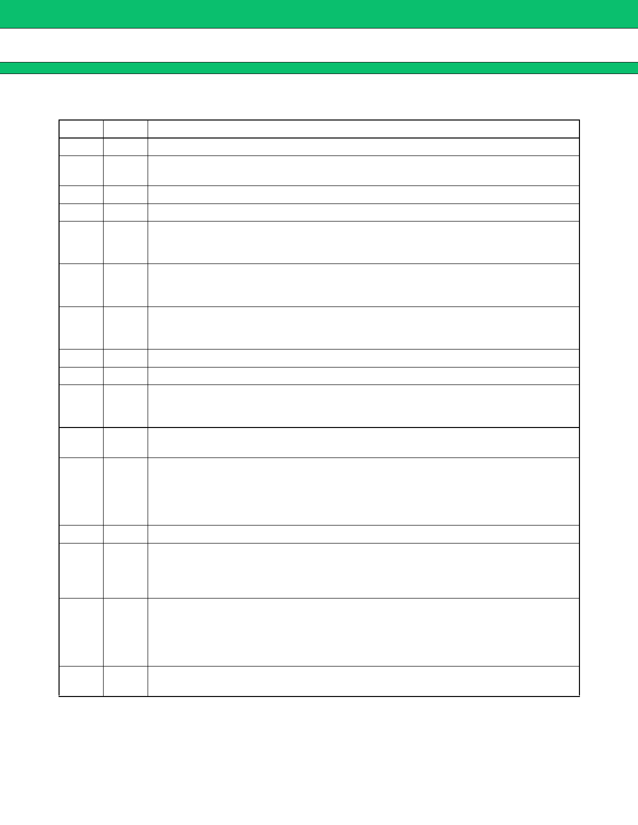
■ PIN DESCRIPTION
No.
Pin
Function
1
CT Oscillator timing capacitor terminal (150 pF to 15,000 pF) .
2
RT
Oscillator timing resistor terminal (5.1 kΩ to 100 kΩ) .
VREF × 1/2 voltage is also available at this pin for error amplifier reference input.
3
+IN1 Error amplifier 1 non-inverted input terminal.
4
−IN1 Error amplifier 1 inverted input terminal.
Error amplifier 1 output terminal.
5
FB1 A resistor and a capacitor are connected between this terminal and the −IN1 terminal to adjust
gain and frequency.
OUT1 dead-time control terminal.
6
DTC1 Dead-time control is adjusted by an external resistive divider connected to the VREF pin.
A capacitor connected between this terminal and GND enables soft-start operation.
Open collector output terminal.
7
OUT1 Output transistor has common ground independent of signal ground.
This output can source or sink up to 50 mA.
8 E/GND Ground terminal.
9
VCC Power supply terminal (3.6 V to 18 V)
Open collector output terminal.
10 OUT2 Output transistor has common ground independent of signal ground.
This output can source or sink up to 50 mA.
11
DTC2
Sets the dead-time of OUT2.
The use of this terminal is the same as that of DTC1.
Error amplifier 2 output terminal.
Sets the gain and adjusts the frequency when a resistor and a capacitor are connected
12
FB2 between this terminal and the −IN2 terminal.
Voltage of VREF × 1/2 voltage is internally connected to the non-inverted input of error amplifier
2. Uses error amplifier 2 for positive voltage output.
13
−IN2 Error amplifier 2 inverted input terminal.
Power control terminal.
14
CTL
The IC is set in the stand-by state when this terminal is set “Low.”
Current consumption is 10 µA or lower in the stand-by state.
The input can be driven by TTL or CMOS.
The time constant setting capacitor connection terminal of the timer latch short-circuit
protection circuit.
15
SCP Connects a capacitor between this pin and GND.
For details, see “■ HOW TO SET TIME CONSTANT FOR TIMER LATCH SHORT-CIRCUIT
PROTECTION CIRCUIT”.
16
VREF
2.46 V reference voltage output terminal which can be obtained up to 1 mA.
This pin is used to set the reference input and idle period of the error amplifiers.
3
Share Link: 