A62S7332E-5 Просмотр технического описания (PDF) - AMIC Technology
Номер в каталоге
Компоненты Описание
Список матч
A62S7332E-5
AMIC Technology

A62S7332E-5 Datasheet PDF : 17 Pages
| |||
A63G7332 Series
Notes: 1. X = "Disregard", H = Logic High, L = Logic Low.
2. WRITE = L means:
1) Any BWx ( BW1 , BW2 , BW3 , or BW4 ) and BWE are low or
2) GW is low.
3. All inputs except OE must be synchronized with setup and hold times around the rising edge (L-H) of CLK.
4. For write cycles that follow read cycles, OE must be HIGH before the input data request setup time and held
HIGH throughout the input data hold time.
5. ADSP LOW always initiates an internal Read at the L-H edge of CLK. A Write is performed by setting one or
more byte write enable signals and BWE LOW or GW LOW for the subsequent L-H edge of CLK. Refer to
the Write timing diagram for clarification.
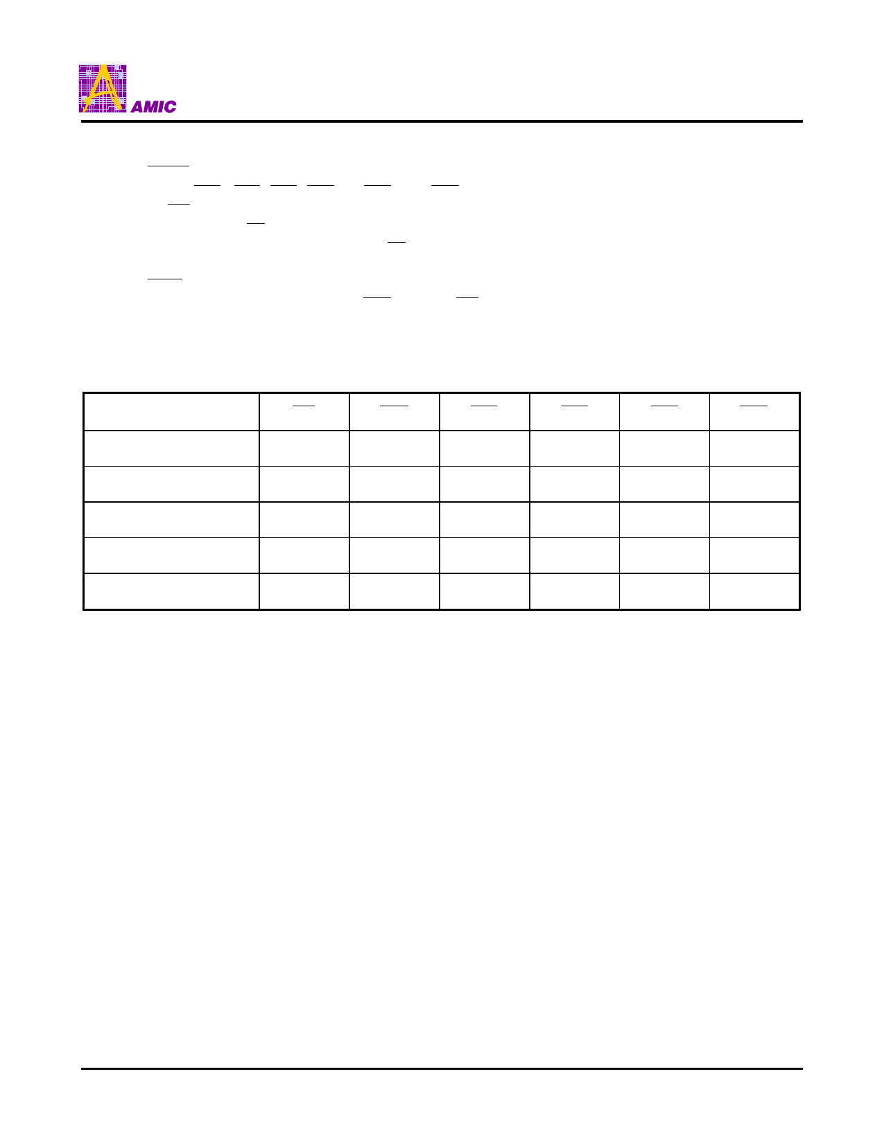
Write Truth Table
Operation
READ
READ
WRITE Byte 1
WRITE all bytes
WRITE all bytes
GW
BWE
BW1
BW2
BW3
BW4
H
H
X
X
X
X
H
L
H
H
H
H
H
L
L
H
H
H
H
L
L
L
L
L
L
X
X
X
X
X
PRELIMINARY (December, 1998, Version 2.1)
6
AMIC Technology, Inc.
Share Link: