A62S7332E-5 Просмотр технического описания (PDF) - AMIC Technology
Номер в каталоге
Компоненты Описание
Список матч
A62S7332E-5
AMIC Technology

A62S7332E-5 Datasheet PDF : 17 Pages
| |||
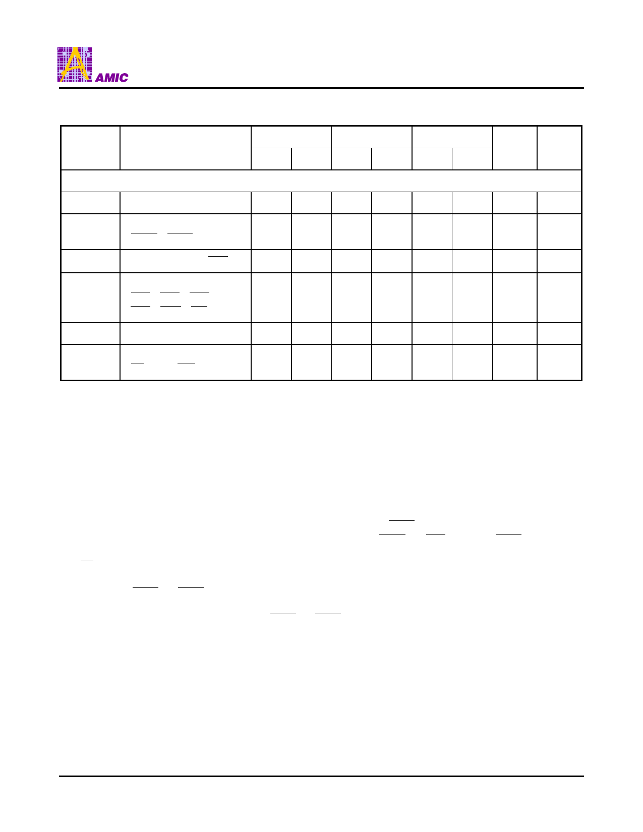
A63G7332 Series
AC Characteristics (continued)
Symbol
Parameter
Hold Times
tAH
Address
tADVH
Address Status
( ADSC , ADSP )
tAAH
Address Advance ( ADV )
tWH
Write Signal
( BW1 , BW2 , BW3 ,
BW4 , BWE , GW )
tDH
Data-in
tCEH
Chip Enable
( CE , CE2, CE2 )
-4.2
-4.5
-5.0
Unit
Min. Max. Min. Max. Min. Max.
Note
0.5
-
0.5
-
0.5
-
0.5
-
0.5
-
0.5
-
0.5
-
0.5
-
0.5
-
0.5
-
0.5
-
0.5
-
ns
7, 9
ns
7, 9
ns
7, 9
ns
7, 9
0.5
-
0.5
-
0.5
-
0.5
-
0.5
-
0.5
-
ns
7, 9
ns
7, 9
Notes:
1. All voltages refer to GND.
2. Overshoot: VIH ≤+4.6V for t ≤tKC/2.
Undershoot: VIH ≥ -0.7V for t ≤tKC/2.
Power-up: VIH ≤+3.6 and VCC ≤3.1V
for t ≤ 200ms
3. ICC is given with no output current. ICC increases with greater output loading and faster cycle times.
4. Test conditions assume the output loading shown in Figure 1, unless otherwise specified.
5. For output loading, CL = 5pF, as shown in Figure 2. Transition is measured ±150mV from steady state voltage.
6. At any given temperature and voltage condition, tKQHZ is less than tKQLZ and tOEHZ is less than tQELZ.
7. A WRITE cycle is defined by at least one Byte Write enable LOW and ADSP HIGH for the required setup and hold
times. A READ cycle is defined by all byte write enables HIGH and ( ADSC or ADV LOW) or ADSP LOW for the
required setup and hold times.
8. OE has no effect when a Byte Write enable is sampled LOW.
9. This is a synchronous device. All addresses must meet the specified setup and hold times for all rising edges of CLK
when either ADSP or ADSC is LOW and the chip is enabled. All other synchronous inputs must meet the setup and
hold times with stable logic levels for all rising edges of clock (CLK) when the chip is enabled. Chip enable must be
valid at each rising edge of CLK when either ADSP or ADSC is LOW to remain enabled.
10. The load used for VOH, VOL testing is shown in Figure 2. AC load current is higher than the given DC values.
AC I/O curves are available upon request.
11. "Device Deselected" means device is in POWER-DOWN mode, as defined in the truth table. "Device Selected" means
device is active (not in POWER-DOWN mode).
12. MODE pin has an internal pulled-up, and ZZ pin has an internal pulled-down. All of then exhibit an input leakage
current of 10µA.
13. Snooze (ZZ) input is recommended that users plan for four clock cycles to go into SLEEP mode and four clocks to
emerge from SLEEP mode to ensure no data is lost.
PRELIMINARY (December, 1998, Version 2.1)
10
AMIC Technology, Inc.
Share Link: