M38C88EA-XXXFP Просмотр технического описания (PDF) - MITSUBISHI ELECTRIC
Номер в каталоге
Компоненты Описание
Список матч
M38C88EA-XXXFP Datasheet PDF : 51 Pages
| |||
PRELIMINARY NSocothimcaene:gpTeah.riasmisetnrioct laimfiintsalasrepescuibfijceacttioton.
MITSUBISHI MICROCOMPUTERS
38C8 Group
SINGLE-CHIP 8-BIT CMOS MICROCOMPUTER
Timer X
Timer X is a 16-bit timer that can be selected in one of four modes
and can be controlled the timer X write by setting the timer X mode
register.
(1) Timer Mode
When the timer X count source selection bit is “0”, the timer counts
f(XIN)/16 (or f(XCIN)/16 in low-speed mode). When it is “1”, the timer
counts f(XIN).
(2) Buzzer Output Mode
Each time the timer underflows, a signal output from the BEEP+ pin
is inverted. When the BEEP- valid bit is “1”, the opposite phase of
BEEP+ signal is output from the BEEP- pin. When using the BEEP+
pin and the BEEP- pin, set ports shared with these pins to output.
(3) Event Counter Mode
The timer counts signals input through the CNTR0 pin.
Except for this, the operation in event counter mode is the same as
in timer mode. When using a timer in this mode, set the port shared
with the CNTR0 pin to input.
(4) Pulse Width Measurement Mode
When the timer X count source selection bit is “0”, the count source
is f(XIN)/16 (or f(XCIN)/16 in low-speed mode). When it is “1”, the
count source is f(XIN).
If CNTR0 active edge switch bit is “0”, the timer counts while the
input signal of CNTR0 pin is at “H”. If it is “1”, the timer counts while
the input signal of CNTR0 pin is at “L”. When using a timer in this
mode, set the port shared with the CNTR0 pin to input.
qTimer X write control
If the timer X write control bit is “0”, when the value is written in the
address of timer X, the value is loaded in the timer X and the latch
at the same time.
If the timer X write control bit is “1”, when the value is written in the
address of timer X, the value is loaded only in the latch. The value
in the latch is loaded in timer X after timer X underflows.
If the value is written in latch only, unexpected value may be set in
the high-order counter when the writing in high-order latch and the
underflow of timer X are performed at the same timing.
sNotes on CNTR0 interrupt active edge selection
CNTR0 interrupt active edge depends on the CNTR0 active edge
switch bit.
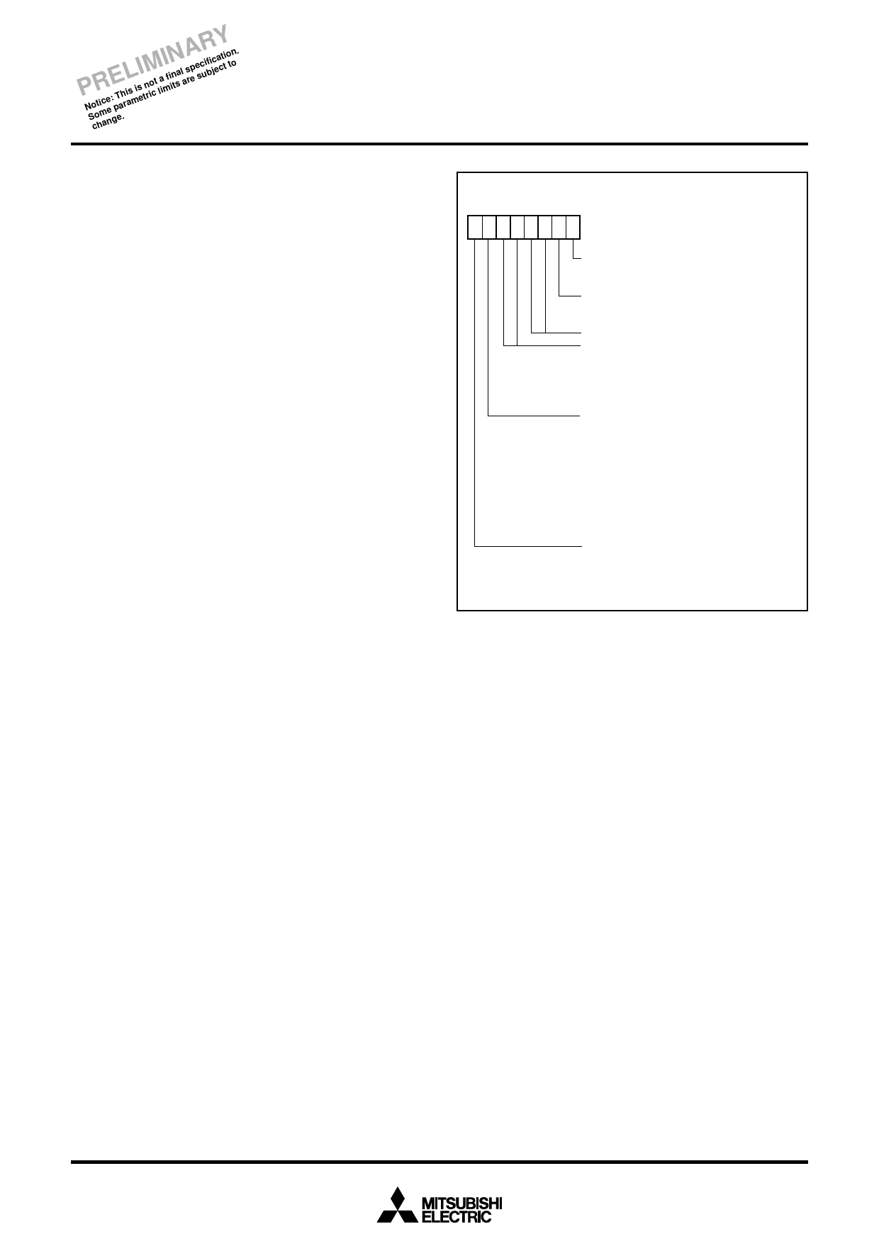
b7
b0
Timer X mode register
(TXM : address 002716)
Timer X write control bit
0 : Write value in latch and counter
1 : Write value in latch only
BEEP- valid bit
0 : Invalid
1 : Valid
Not used
Timer X operating mode bits
b5 b4
0 0 : Timer mode
0 1 : Buzzer output mode
1 0 : Event counter mode
1 1 : Pulse width measurement mode
CNTR0 active edge switch bit
0 : Count at rising edge in event counter mode
Start from “H” output in pulse output mode
Measure “H” pulse width in pulse width
measurement mode
Falling edge active for interrupt
1 : Count at falling edge in event counter mode
Start from “L” output in pulse output mode
Measure “L” pulse width in pulse width
measurement mode
Rising edge active for interrupt
Timer X stop control bit
0 : Count start
1 : Count stop
Fig. 17 Structure of timer X mode register
21
Share Link: 