LX8415-00(2005) Просмотр технического описания (PDF) - Microsemi Corporation
Номер в каталоге
Компоненты Описание
Список матч
LX8415-00 Datasheet PDF : 7 Pages
| |||
PRODUCT DATABOOK 1996/1997
0.5A LOW DROPOUT POSITIVE REGULATORS
PR E L I M I N A RY D ATA S H E E T
LX8415-xx
APPLICATION NOTES
OUTPUT VOLTAGE
LOAD REGULATION (continued)
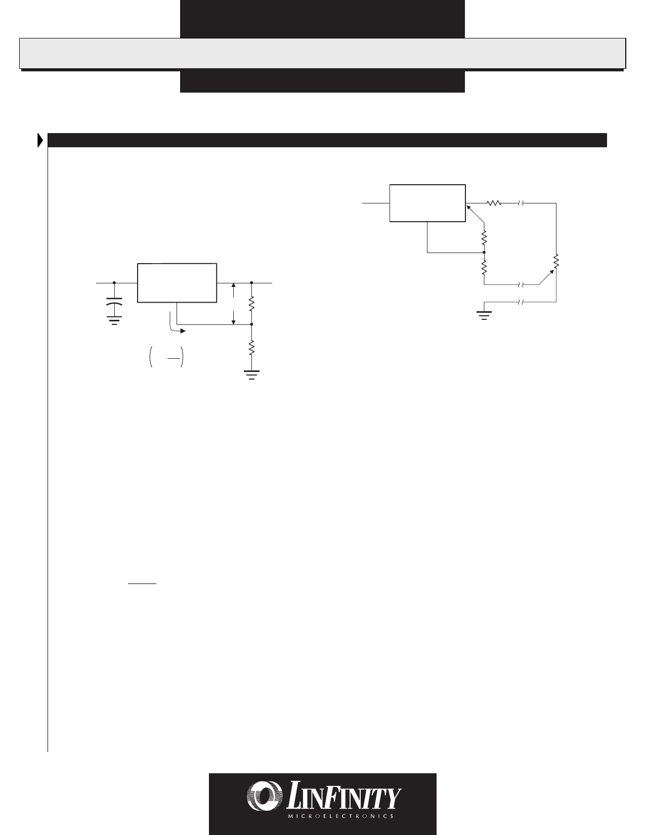
The LX8415 ICs develop a 1.25V reference voltage between the output
RP
and the adjust terminal (See Figure 2). By placing a resistor, R1,
LX8415-xx
Parasitic
Line Resistance
between these two terminals, a constant current is caused to flow
VIN
IN
OUT
through R1 and down through R2 to set the overall output voltage.
Normally this current is the specified minimum load current of 10mA.
Because I is very small and constant when compared with the current
ADJ
through R1, it represents a small error and can usually be ignored.
LX8415-xx
VIN
IN
OUT
e ADJ
VREF
IADJ
t 50µA
VOUT = VREF
1
+
R2
R1
+ IADJ R2
VOUT
R1
R2
le FIGURE 2 — BASIC ADJUSTABLE REGULATOR
LOAD REGULATION
Because the LX8415 regulators are three-terminal devices, it is not
possible to provide true remote load sensing. Load regulation will
o be limited by the resistance of the wire connecting the regulator to
the load. The data sheet specification for load regulation is
measured at the bottom of the package. Negative side sensing is a
true Kelvin connection, with the bottom of the output divider
returned to the negative side of the load. Although it may not be
s immediately obvious, best load regulation is obtained when the top
of the resistor divider, (R1), is connected directly to the case of the
regulator, not to the load. This is illustrated in Figure 3. If R1 were
connected to the load, the effective resistance between the regulator
and the load would be:
b RPeff
=
R
P
*
R2+R1
R1
where: R ≡ Actual parasitic line resistance.
P
O When the circuit is connected as shown in Figure 3, the parasitic
ADJ
Connect
R1 to Case
of Regulator
R1
R2
RL
Connect
R2
to Load
FIGURE 3 — CONNECTIONS FOR BEST LOAD REGULATION
is important to keep the connection between the regulator output
pin and the load as short as possible, and to use wide traces or
heavy-gauge wire.
The minimum specified output capacitance for the regulator
should be located near the reglator package. If several capacitors
are used in parallel to construct the power system output capaci-
tance, any capacitors beyond the minimum needed to meet the
specified requirements of the regulator should be located near the
sections of the load that require rapidly-changing amounts of
current. Placing capacitors near the sources of load transients will
help ensure that power system transient response is not impaired
by the effects of trace impedance.
To maintain good load regulation, wide traces should be used on
the input side of the regulator, especially between the input
capacitors and the regulator. Input capacitor ESR must be small
enough that the voltage at the input pin does not drop below V
IN (MIN)
during transients.
V = V + V IN (MIN)
OUT
DROPOUT (MAX)
where:
VIN (MIN)
≡ the lowest allowable instantaneous
voltage at the input pin.
VOUT
≡ the designed output voltage for the
power supply system.
V
≡ the specified dropout voltage
DROPOUT (MAX)
resistance appears as its actual value, rather than the higher R .
Peff
for the installed regulator.
Even when the circuit is optimally configured, parasitic resistance
can be a significant source of error. A 100 mil (2.54 mm) wide PC
THERMAL CONSIDERATIONS
trace built from 1 oz. copper-clad circuit board material has a The LX8415 regulators have internal power and thermal limiting
parasitic resistance of about 5 milliohms per inch of its length at circuitry designed to protect each device under overload conditions.
room temperature. If a 3-terminal regulator used to supply 2.50 volts For continuous normal load conditions, however, maximum junc-
is connected by 2 inches of this trace to a load which draws 5 amps tion temperature ratings must not be exceeded. It is important to
of current, a 50 millivolt drop will appear between the regulator and give careful consideration to all sources of thermal resistance from
the load. Even when the regulator output voltage is precisely junction to ambient. This includes junction to case, case to heat sink
2.50 volts, the load will only see 2.45 volts, which is a 2% error. It interface, and heat sink thermal resistance itself.
Copyright © 1999
Rev. 0.5
5
Share Link: 