LT3645 Просмотр технического описания (PDF) - Linear Technology
Номер в каталоге
Компоненты Описание
Список матч
LT3645 Datasheet PDF : 24 Pages
| |||
LT3645
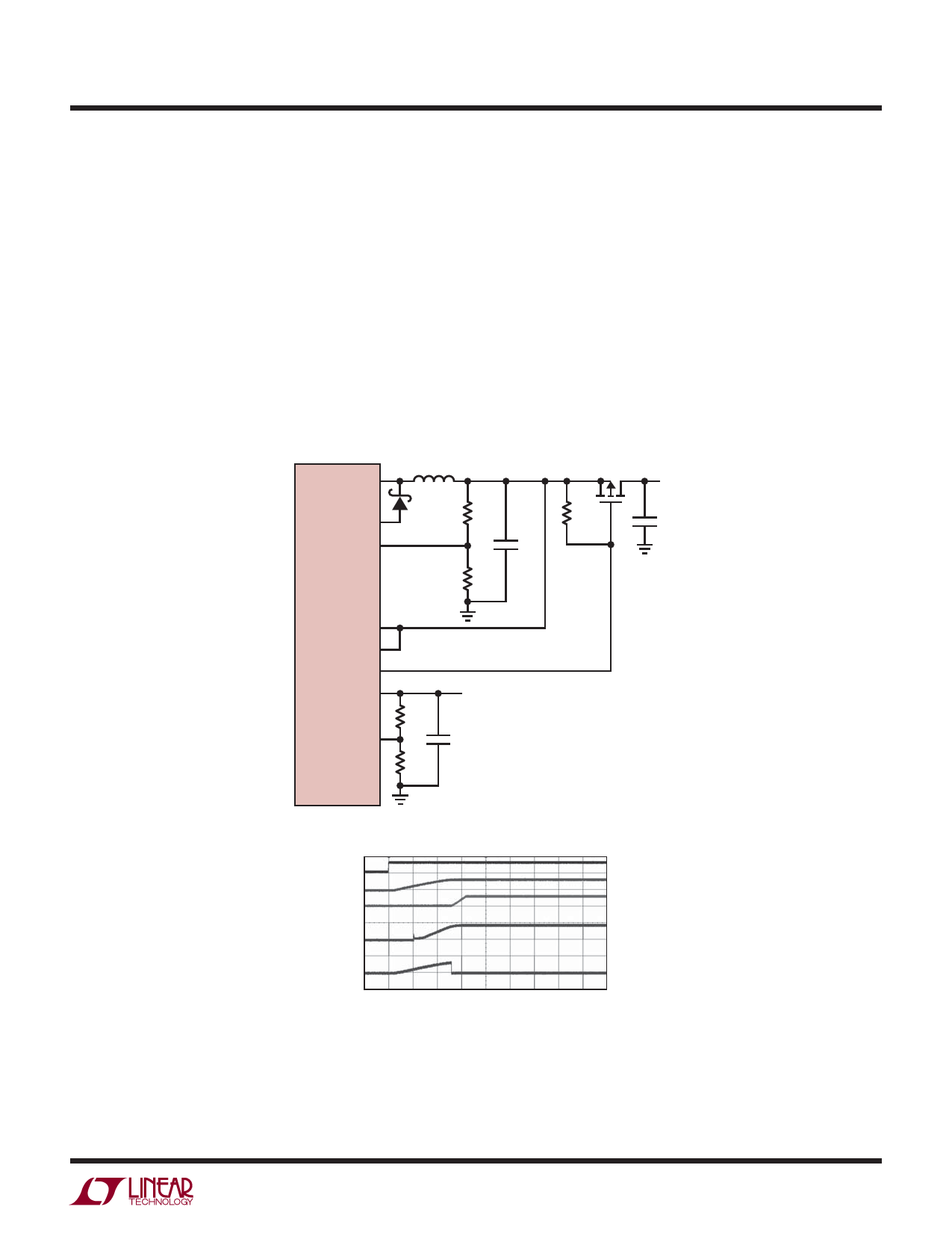
APPLICATIONS INFORMATION
there is a small delay before OUT2 begins ramping up as
OUT2 has to wait until VCC2 is above 2V before power can
be supplied to OUT2.
Figure 12 utilizes the NPG pin to sequence the outputs such
that OUT1 comes into regulation after OUT2 is already in
regulation. When the part is off, the buck output, OUT1
and OUT2 will be 0V. The NPG pin will be high impedance,
PFET P1 will be off and OUT1 will be disconnected from
the buck output. When the part is turned on, first the buck
output will come up to 3.3V. Once the Buck output is in
regulation, the LDO output, OUT2 will come up to 1.8V.
When both OUT2 and the buck output are in regulation,
the NPG pin will pull low, turning on PFET P1 and sup-
plying power to OUT1.
The NPG pin is capable of sinking 1mA and will pull the
gate of P1 down to 300mV. Therefore R9 should be chosen
such that:
R9 < (VOUT1 – 300mV)/1mA
Where R7 is in Ω. For a 3.3V buck output application,
PFET P1 must be able to source 300mA to OUT1 from
the buck output with ~3V of gate drive. Note that PFET
SW
LT3645
DA
FB
4.7μH
BUCK OUTPUT
P1
31.6K
10μF
R9
31.6K
10K
OUT1
0.1μF
VCC2
EN2
NPG
OUT2
FB2
12.4k
10k
OUT2
2.2μF
3645 F12
EN/UVLO, 20V/DIV
BUCK OUTPUT, 5V/DIV
OUT1, 5V/DIV
OUT2
2V/DIV
NPG
5V/DIV
500μs/DIV
Figure 12. OUT2 Comes Up Before OUT1
3645f
17
Share Link: 