LT3645 Просмотр технического описания (PDF) - Linear Technology
Номер в каталоге
Компоненты Описание
Список матч
LT3645 Datasheet PDF : 24 Pages
| |||
LT3645
APPLICATIONS INFORMATION
temperature range. The X5R and X7R dielectrics result in
more stable characteristics and are more suitable for use
as the output capacitor. The X7R type has better stability
across temperature, while the X5R is less expensive and
is available in higher values. Care still must be exercised
when using X5R and X7R capacitors; the X5R and X7R
codes only specify operating temperature range and maxi-
mum capacitance change over temperature. Capacitance
change due to DC bias with X5R and X7R capacitors
is better than Y5V and Z5U capacitors, but can still be
significant enough to drop capacitor values below ap-
propriate levels. Capacitor DC bias characteristics tend to
improve as component case size increases, but expected
capacitance at operating voltage should be verified. Voltage
and temperature coefficients are not the only sources of
problems. Some ceramic capacitors have a piezoelectric
response. A piezoelectric device generates voltage across
its terminals due to mechanical stress, similar to the way
a piezoelectric microphone works. For a ceramic capacitor
the stress can be induced by vibrations in the system or
thermal transients.
Precision Undervoltage Lockout
The EN/UVLO pin has an accurate 1.23V threshold that
can be used to shutdown the part when the input voltage
drops below a specified level. To perform this function, a
resistor divider between the EN/UVLO pin and the VIN pin
can be tied as shown in Figure 10. The resistor values can
be determined from the following equation:
R7
"
R8 t
©
ǻ
VIN(MIN)
1.23V
–
1¹»º
With the resistor divider connected, the part will only
operate at input voltages greater than VIN(MIN). Note that
the resistor divider will always draw current from VIN. To
reduce this current, the user might use large value resis-
tors for R7 and R8. This is acceptable as long as R7 and
R8 are selected such that they can supply 10μA to the
EN/UVLO pin. A good value for R8 is 100k.
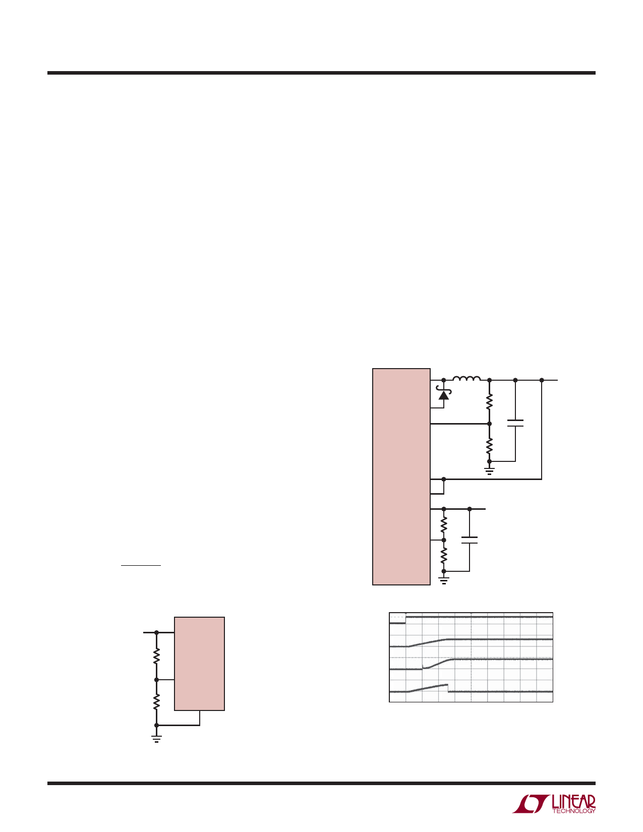
Output Voltage Sequencing
There are a few applications available for sequencing the
buck and LDO output voltages. In Figures 11 and 12, the
buck output (OUT1) is programmed to 3.3V, while the LDO
output (OUT2) is programmed to 1.8V.
Figure 11 shows a standard configuration where OUT1 and
OUT2 come up as soon as possible. In this configuration,
SW
LT3645
DA
FB
4.7μH
31.6K
10μF
10K
OUT1
VCC2
EN2
OUT2
FB2
12.4k
10k
OUT2
2.2μF
3645 F11
VIN
VIN
LT3645
R7
EN/UVLO
R8
GND
3645 F10
Figure 10. Precision UVLO Circuit
16
EN/UVLO
20V/DIV
OUT1
5V/DIV
OUT2
2V/DIV
NPG
5V/DIV
500μs/DIV
Figure 11. OUT1 and OUT2 Come Up as Soon as Possible
3645f
Share Link: 