LT3645 Просмотр технического описания (PDF) - Linear Technology
Номер в каталоге
Компоненты Описание
Список матч
LT3645 Datasheet PDF : 24 Pages
| |||
LT3645
APPLICATIONS INFORMATION
FB Resistor Networks
The output voltages are programmed with resistor dividers
between the outputs and the VFB and VFB2 pins. Choose
the resistors according to
R1" R2 t
©
ǻ
VOUT
0.8
– 1¹»º
R3
"
R4
t
©
ǻ
VOUT2
0.797
–
1¹»º
R2 and R4 should be 20k or less to avoid bias current
errors. In the step-down converter, an optional phase
lead capacitor of 22pf between VOUT and VFB reduces
light-load ripple.
voltages up to 55V, but once the input voltage exceeds
36V, the power switch will shut off and stop regulating
the output voltage until the input voltage falls below 36V.
Minimum On Time
The LT3645 will operate at the correct frequency while
the input voltage is below VIN(MAX). At input voltages
that exceed VIN(MAX), the LT3645 will still regulate the
output properly (up to 38.5V); however, the LT3645 will
skip pulses to regulate the output voltage resulting in
increased output voltage ripple.
Figure 1 illustrates switching waveforms for a LT3645
application with VOUT = 1.2V near VIN(MAX) = 21.3V.
Input Voltage Range
The maximum operating input voltage for the LT3645 is
36V. The minimum input voltage is determined by either
the LT3645’s minimum operating voltage of 3.6V or by
its maximum duty cycle. The duty cycle is the fraction of
time that the internal switch is on and is determined by
the input and output voltages:
DC = (VOUT + VD)/(VIN – VSW + VD)
where VD is the forward voltage drop of the catch diode
(~0.4V) and VSW is the voltage drop of the internal switch
(~0.4V at maximum load). This leads to a minimum input
voltage of:
VIN(MIN) = ((VOUT + VD)/DCMAX) – VD + VSW
with DCMAX = 0.83 for the LT3645.
The maximum input voltage is determined by the absolute
maximum ratings of the VIN and BOOST pins. For fixed
frequency operation, the maximum input voltage is de-
termined by the minimum duty cycle, which is:
VIN(MAX) = ((VOUT + VD)/DCMIN) – VD + VSW
with DCMIN = 0.075 for the LT3645.
Note that this is a restriction on the operating input voltage
for continuous mode operation. The circuit will continue
to regulate the output up until the overvoltage lockout
input voltage (38.5V). The part will tolerate transient input
SWITCH
VOLTAGE
10V/DIV
INDUCTOR
CURRENT
0.5A/DIV
VIN = 18V
VOUT = 1.2V
IOUT = 500mA
COUT = 10μF
L = 10μH
Figure 1.
3645 F01
As the input voltage is increased, the part is required
to switch for shorter periods of time. Delays associated
with turning off the power switch dictate the minimum on
time of the part. The minimum on time for the LT3645 is
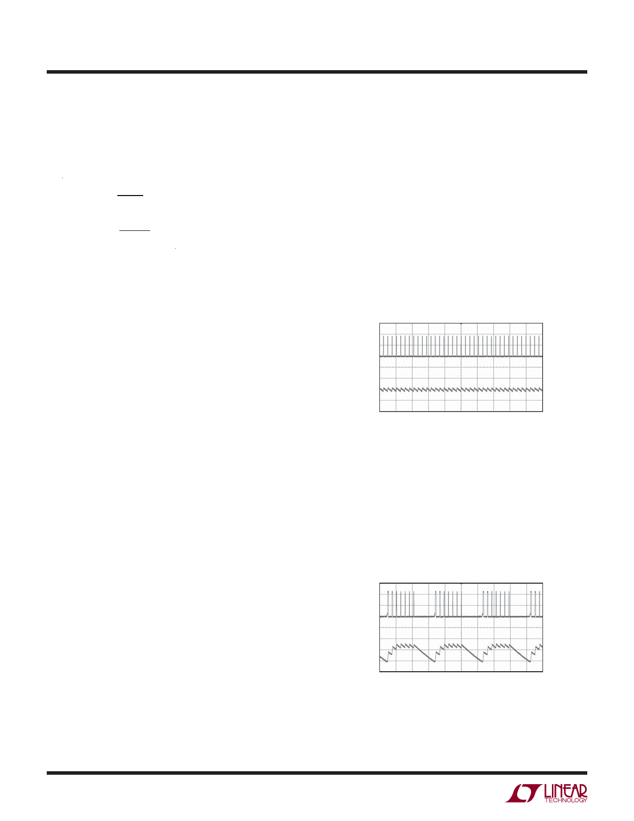
100ns. Figure 2 illustrates the switching waveforms when
the input voltage is increased to VIN = 22V.
SWITCH
VOLTAGE
10V/DIV
INDUCTOR
CURRENT
0.5A/DIV
VIN = 22V
VOUT = 1.2V
IOUT = 500mA
COUT = 10μF
L = 10μH
Figure 2.
3645 F02
3645f
10
Share Link: 