LIS331DL Просмотр технического описания (PDF) - STMicroelectronics
Номер в каталоге
Компоненты Описание
Список матч
LIS331DL
STMicroelectronics

LIS331DL Datasheet PDF : 42 Pages
| |||
Digital interfaces
LIS331DL
Table 13. Transfer when Master is receiving (reading) one byte of data from slave
Master ST SAD + W
SUB
SR SAD + R
NMAK SP
Slave
SAK
SAK
SAK DATA
Table 14. Transfer when Master is receiving (reading) multiple bytes of data from slave
Master ST SAD+W
SUB
SR SAD+R
MAK
MAK
NMAK SP
Slave
SAK
SAK
SAK DATA
DATA
DATA
Data are transmitted in byte format (DATA). Each data transfer contains 8 bits. The number
of bytes transferred per transfer is unlimited. Data is transferred with the Most Significant bit
(MSb) first. If a receiver can’t receive another complete byte of data until it has performed
some other function, it can hold the clock line, SCL LOW to force the transmitter into a wait
state. Data transfer only continues when the receiver is ready for another byte and releases
the data line. If a slave receiver doesn’t acknowledge the slave address (i.e. it is not able to
receive because it is performing some real time function) the data line must be left HIGH by
the slave. The Master can then abort the transfer. A LOW to HIGH transition on the SDA line
while the SCL line is HIGH is defined as a STOP condition. Each data transfer must be
terminated by the generation of a STOP (SP) condition.
In order to read multiple bytes, it is necessary to assert the most significant bit of the sub-
address field. In other words, SUB(7) must be equal to 1 while SUB(6-0) represents the
address of first register to be read.
In the presented communication format MAK is Master Acknowledge and NMAK is No
Master Acknowledge.
5.2
SPI bus interface
The LIS331DL SPI is a bus slave. The SPI allows to write and read the registers of the
device.
The Serial Interface interacts with the outside world with 4 wires: CS, SPC, SDI and SDO.
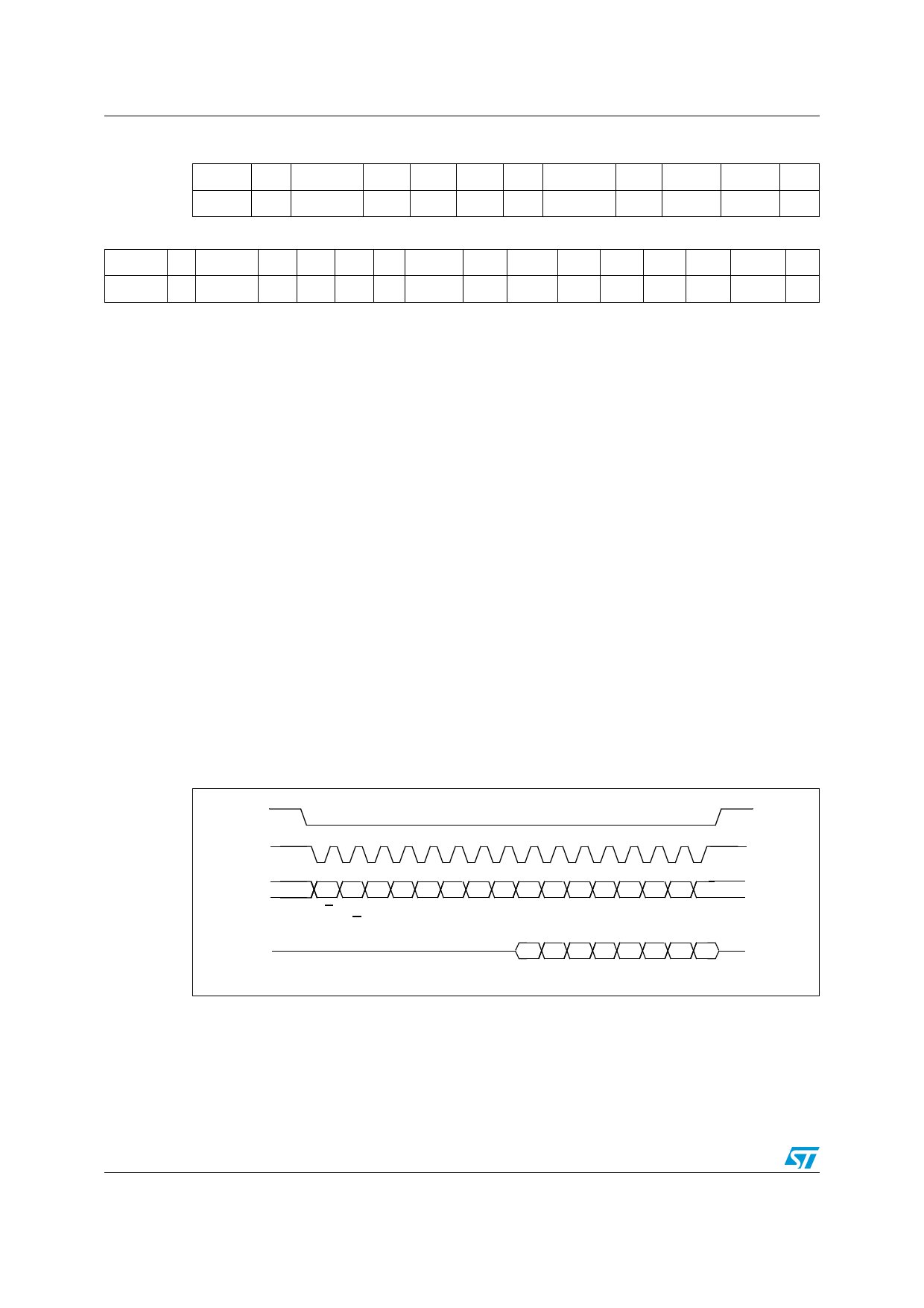
Figure 6. Read & write protocol
CS
SPC
SDI
SDO
RW
DI7 DI6 DI5 DI4 DI3 DI2 DI1 DI0
MS AD5 AD4 AD3 AD2 AD1 AD0
DO7 DO6 DO5 DO4 DO3 DO2 DO1 DO0
CS is the Serial Port Enable and it is controlled by the SPI master. It goes low at the start of
the transmission and goes back high at the end. SPC is the Serial Port Clock and it is
controlled by the SPI master. It is stopped high when CS is high (no transmission). SDI and
SDO are respectively the Serial Port Data Input and Output. Those lines are driven at the
falling edge of SPC and should be captured at the rising edge of SPC.
20/42
Share Link: