LAN91C96 Просмотр технического описания (PDF) - SMSC -> Microchip
Номер в каталоге
Компоненты Описание
Список матч
LAN91C96 Datasheet PDF : 125 Pages
| |||
Non-PCI Single-Chip Full Duplex Ethernet Controller with Magic Packet
The LAN91C96 consists of an integrated Ethernet controller mapped entirely in I/O space. In addition,
PCMCIA attribute memory space is decoded to interface an external CIS ROM, with configuration registers as
per PCMCIA 3.X extensions (except COR) implemented on-chip in attribute space above the ROM decode
area. The PCMCIA Configuration Registers are accessible in I/O space and also to allow non-PCMCIA dual
function designs.
The Ethernet controller function includes a built-in 6kbyte RAM for packet storage. This RAM buffer is
accessed by the CPU through sequential access regions of 256 bytes each. The RAM access is internally
arbitrated by the LAN91C96, and dynamically allocated between transmit and receive packets. Each packet
may consist of one or more 256 byte page. The Ethernet controller functionality is identical to the LAN91C94
and LAN91C95 except where indicated otherwise.
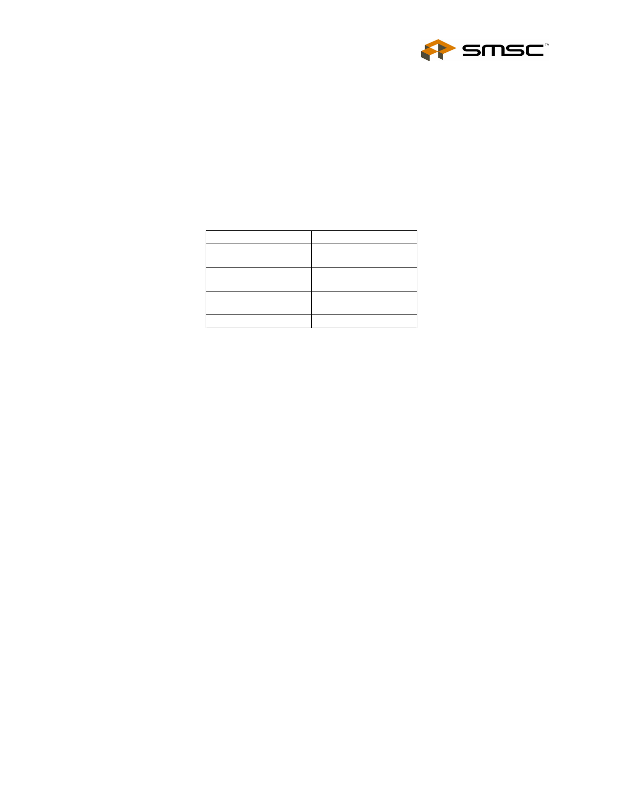
The LAN91C96 Memory Management Unit parameters are:
RAM SIZE
MAX. NUMBER OF
PAGES
MAX. NUMBER OF
PACKETS
MAX. PAGES PER
PACKET
PAGE SIZE
6kbytes
24
24 (FIFOs have 24
entries of 5 bits)
6
256 bytes
5.1
Buffer Memory
The logical addresses for RAM access are divided into TX area and RX area.
The TX area is seen by the CPU as a window through which packets can be loaded into memory before
queuing them in the TX FIFO of packets. The TX area can also be used to examine the transmit
completion status after packet transmission.
The RX area is associated to the output of the RX FIFO of packets, and is used to access receive packet
data and status information.
The logical address is specified by loading the address pointer register. The pointer can automatically
increment on accesses.
All accesses to the RAM are done via I/O space.
A bit in the address pointer also specifies if the address refers to the TX or RX area.
In the TX area, the host CPU has access to the next transmit packet being prepared for transmission. In
the RX area, it has access to the first receive packet not processed by the CPU yet.
The FIFO of packets, existing beneath the TX and RX areas, is managed by the MMU. The MMU
dynamically allocates and releases memory to be used by the transmit and receive functions.
SMSC LAN91C965v&3v
Page 23
DATASHEET
Rev. 09/10/2004
Share Link: 