HA17524P Просмотр технического описания (PDF) - Hitachi -> Renesas Electronics
Номер в каталоге
Компоненты Описание
Список матч
HA17524P Datasheet PDF : 18 Pages
| |||
HA17524P/FP
Q1
6
I
RT
VREF
Q2
Q3
Discharge
7
I CT
VH
∆V
T
VL
CT Terminal Waveform
I ≈ VREF – VEB (Q2) – VEB (Q3)
RT
∆V = VH – VL ≅ 3.8 – 0.9 = 2.9 V
1
T ≈ CT · ∆V · I
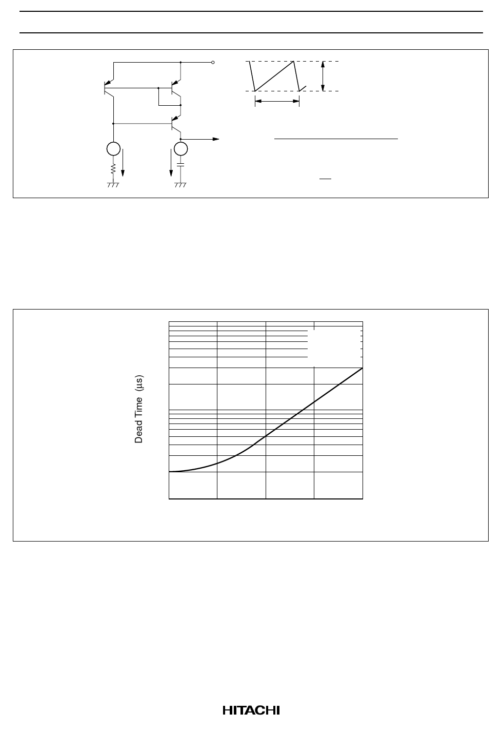
Figure 4 Oscillating Circuit and CT Terminal Waveform
The oscillator output pulse signal is used as the flip flop clock pulse and as switching pulses for the output
transistors, synchronous to the clock pulse.
The pulse-widths which can be controlled by the timing capacitor CT as shown in figure 5, increases output
dead time.
10
VCC = 20 V
RT = 10 kΩ
Ta = 25°C
3
1.0
0.3
0.1
0.001 0.003
0.01
0.03
0.1
Timing Capacitance CT (µF)
Figure 5 Dead Time vs Timing Capacitance
Reference Voltage: The built-in regulator (reference voltage: VREF = 5 ±0.4 V) can be used as a reference
power supply for the error amplifier, which determines output voltage (VOUT). It is also connected as a bias
source for another circuits in IC.
5
Share Link: 