HA17524P Просмотр технического описания (PDF) - Hitachi -> Renesas Electronics
Номер в каталоге
Компоненты Описание
Список матч
HA17524P Datasheet PDF : 18 Pages
| |||
HA17524P/FP
Functional Description
Principals of HA17524 Operation
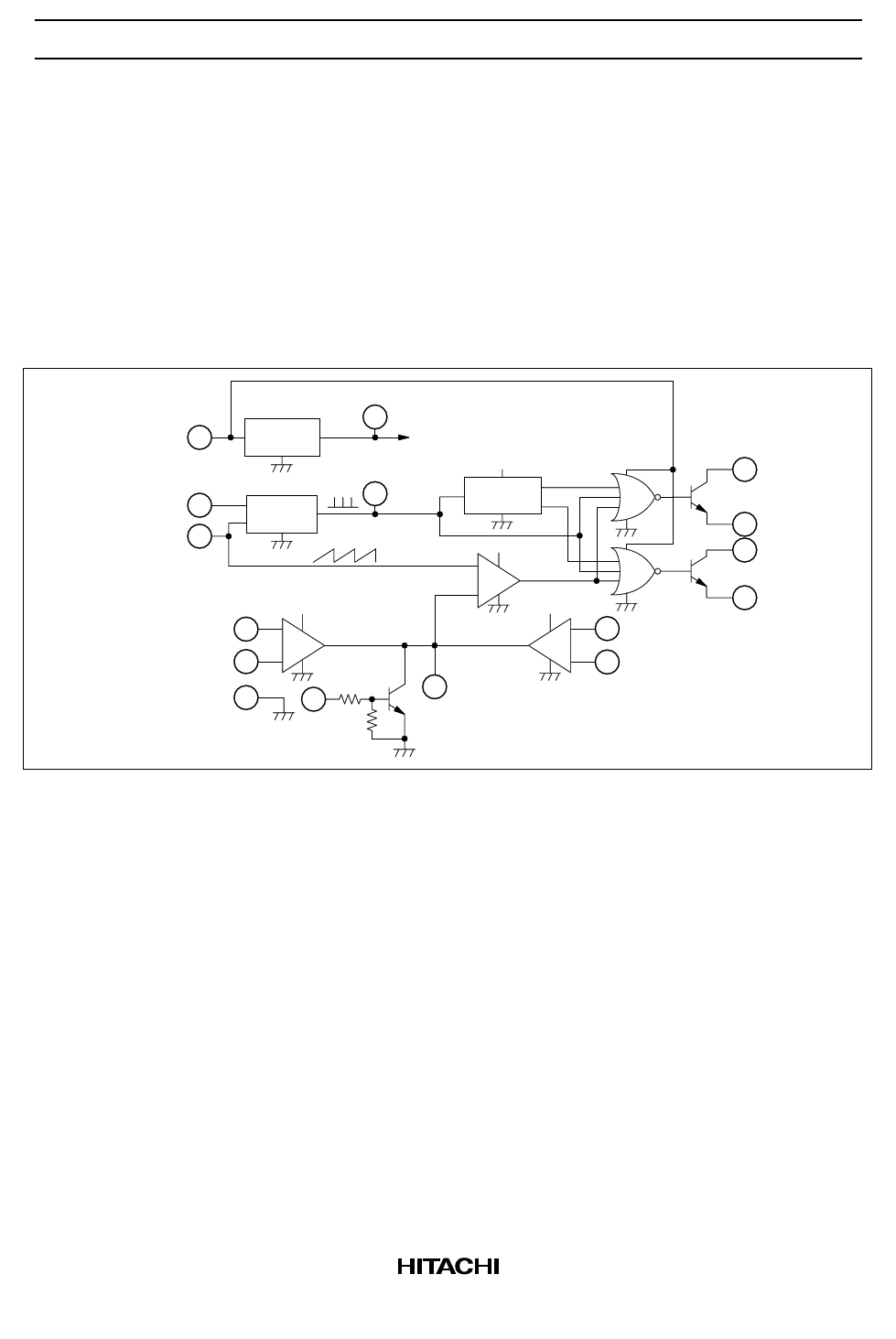
The HA17524 switching regulator circuit, using pulse width modulation (PWM), is constructed as shown
in figure 1.
Timing resistances RT and timing capacitance CT control the oscillation frequency. CT is charged by a
constant current generated by RT. Ramp signals (saw-tooth waves) at the CT terminal generated by this
oscillator is available for reference input signal to comparator which control the pulse width.
VREF
VCC 15
RT 6
CT 7
(Ramp)
Ref.
Volt.
+5 V
Osc.
+5V
16
+5 V to internal circuitry
OSC Out
+5V
Q
3
Flip Flop
NOR
Q
+5V
—
Comparator
NOR
+
+5V
INV. Input 1
NON-INV. Input 2
GND 8
— Error Amp.
+
1kΩ
10
9 COMP
+
C.L.
—
4 CL(+)
5 CL(—)
Current Limiter
SHUT 10kΩ
DOWN
12 C1
Q1
11 E1
13 C2
Q2
14 E2
Figure 1 HA17524 Block Diagram
The reference voltage connects to the non-inverted or inverted input terminal of the error amplifier via
resistance divider (figure 2).
The output voltage from the error amplifier is compared with the ramp signal capacitance CT (figure 1).
The comparator can provide a signal with modulated pulse width.
This signal, then, controls output transistors Q1 and Q2, making an open loop to stabilize output voltage.
Outputs form the error amplifier the current limiter, and the shut-down circuit are connected together at the
comparator, so that an input signal from any one of these circuits can break the output stage.
2
Share Link: 