ISL97645A Просмотр технического описания (PDF) - Intersil
Номер в каталоге
Компоненты Описание
Список матч
ISL97645A Datasheet PDF : 15 Pages
| |||
ISL97645A
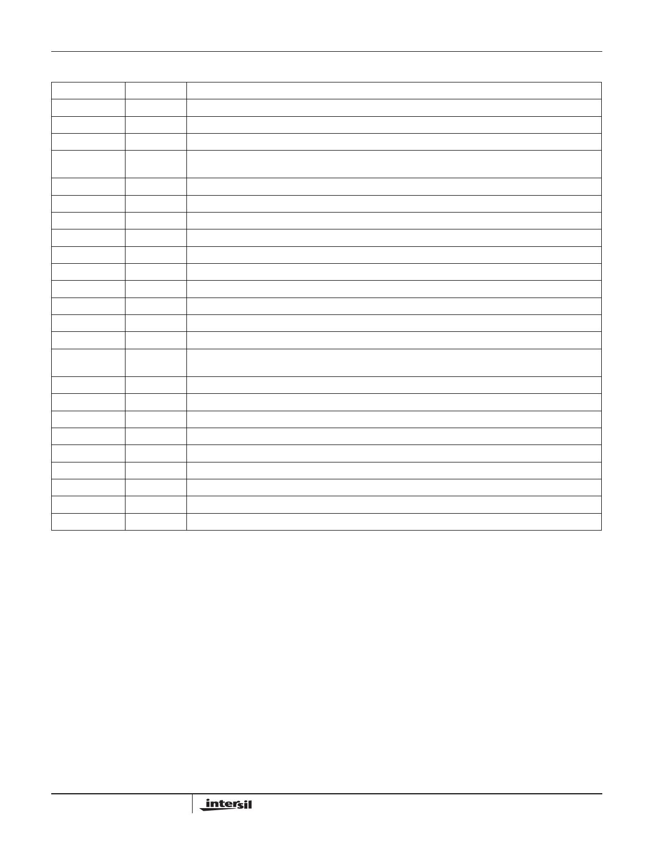
Pin Descriptions
PIN NUMBER
1
2
3
4
NAME
GND
VGH_M
VFLK
VDPM
5
VDD1
6
VDD2
7
OUT
8
NEG
9
POS
10
AGND
11
CD2
12
VDIV
13
RESET
14
SS
15
COMP
16
FREQ
17
VIN2
18
LX
19
ENABLE
20
FB
21
PGND
22
RE
23
CE
24
VGH
DESCRIPTION
Signal ground
Gate Pulse Modulator Output
Gate Pulse Modulator Control input
Gate Pulse Modulator Enable. Connect a capacitor from VDPM to GND to set the delay time before GPM is
enabled. A 20μA current source charges CDPM. Power on delay time = 60.75k*CDPM.
Gate Pulse Modulator Low Voltage Input
VCOM Amplifier Supply
VCOM Amplifier Output
VCOM Amplifier Inverting input
VCOM Amplifier Non-inverting input
VCOM Amplifier Ground
Voltage detector rising edge delay. Connect a capacitor between this pin and GND to set the rising edge delay.
Voltage detector threshold. Connect to the center of a resistive divider between VIN and GND.
Voltage detector reset output.
Boost Converter Soft-Start. Connect a capacitor between this pin and GND to set the soft-start time.
Boost Converter Compensation pin. Connect a series resistor and capacitor between this pin and GND to
optimize transient response.
Boost Converter frequency select
Boost Converter power supply
Boost Converter Switching Node
Chip Enable pin. Connect to VIN1 for normal operation, GND for shutdown.
Boost Converter Feedback
Boost Converter Power Ground
Gate Pulse Modulator Slew Control. Connect a resistor between this pin and GND to set the falling slew rate.
Gate Pulse Modulator Delay Control. Connect a capacitor between this pin and GND to set the delay time.
Gate Pulse Modulator High Voltage Input
2
FN6353.0
July 2, 2007
Share Link: 