IDT821068 Просмотр технического описания (PDF) - Integrated Device Technology
Номер в каталоге
Компоненты Описание
Список матч
IDT821068 Datasheet PDF : 45 Pages
| |||
IDT821068 OCTAL PROGRAMMABLE PCM CODEC
INDUSTRIAL TEMPERATURE RANGE
FUNCTIONAL DESCRIPTION
The IDT821068 performs the CODEC/filter functions required for the
subscribe line interface circuitry in telecommunications system.
IDT821068 converts analog voice signals to digital PCM samples and
digital PCM samples back to analog voice signals. High performance
oversampling Analog-to-Digital Converters (ADC) and Digital-to-
Analog Converters (DAC) in the IDT821068 provide the required
conversion accuracy. The associated decimation and interpolation
filters are realized with both dedicated hardware and Digital Signal
Processor (DSP). The DSP also handles all other necessary functions
such as PCM bandpass filtering, sample rate conversion and PCM
companding. See the Functional Block Diagram for more detail.
MPI/PCM MODE AND GCI MODE
Microprocessor Interface (MPI) and General Control Interface (GCI)
help the user to program and control the CODEC. MPI pin selects the
interface: ‘0’ selects MPI mode and ‘1’ selects GCI mode.
MPI CONTROL MODE
In MPI mode, the internal configuration registers (local/global), the
SLIC signaling interface and the Coefficient-RAM, FSK-RAM of the
IDT821068 are programmed by microprocessor via the serial control
interface, which consists of four lines (pins): CCLK, CS, CI and CO. All
the commands and data transmitted or received are aligned in byte (8
bits). CCLK is the Serial Control Interface Clock, it can be up to 8.192
MHz; CS is the Chip Select pin, a low level on it enables the serial
control interface; CI and CO are the serial control interface data input
and output, carrying the control commands and data bytes to/from the
IDT821068.
The data transfer is synchronized to the CCLK input. The contents
of CI is latched on the rising edges of CCLK, while CO changes on the
falling edges of CCLK. When finishing a read or write command, the
CLCK must last at least one cycle after the CS is set high. During the
execution of commands that are followed by output data (read
commands), the device will not accept any new commands from CI.
The data transfer sequence can be interrupted by setting CS high.
See Figure 1 and Figure 2.
CCLK is the only reference of CI and CO pins. Its duty and
frequency may not necessarily be standard.
PCM BUS
In MPI mode, IDT821068 provides two flexible PCM buses for all 8
channels. The digital PCM data can be compressed (A/µ-law) or
linear format, which is determined by the DMS bit in Global Command
7. The data rate can be configured as same as Bit Clock (BCLK) or
half of it. The data can be transmitted or received either on BCLK
rising edges or on falling edges. The data transmit and receive time
slots can be offset from Frame Synchronization (FS) by 0 BCLK
period to 7 BCLK periods. See Figure 3. All the selections are
implemented by Global Command 7, which is configured for all 8
channels.
The PCM data of each channel can be assigned to any time slot of
the PCM bus. The number of available time slots is determined by
BCLK frequency. For example, when BCLK is 512 kHz, time slot 0-7
are available; when BCLK is 1.024 MHz, time slot 0-15 are available;
when BCLK is 8.192 MHz, time slot 0-127 are available. The
IDT821068 allows any BCLK frequency between 512 kHz and 8.192
MHz at increment of 64 kHz in a system.
When compressed format (8-bit) is selected, the voice data of one
channel occupies one time slot. The TT[6:0] bits in Local Command 7
selects the transmit time slot for each channel, while the RT[6:0] bits in
Local Command 8 selects the receive time slot for each channel.
When linear format is selected, the voice data is a 16-bit 2’s
complement number (b15 and b14 are the same as b13, which is the
sign bit, b13 to b0 are effective bits). Then the voice data of one
channel occupies a time slot group, which is consisted of 2 successive
time slots. The TT[6:0] bits in Local Command 7 select the transmit
time slot group for each channel, while the RT[6:0] bits in Local
Command 8 select the receive time slot group for each channel.
PCM data for each individual channel can be clocked out of DX1 or
DX2 pin on the programmed edges of BCLK according to time slot as-
signment. The transmit highway (DX1/2) is selected by the THS bit in
Local Command 7. The frame sync (FS) pulse identifies the begin-
ning of a transmit frame, or time slot 0. The PCM data is transmitted
serially on DX1 or DX2 with MSB first.
PCM data for each channel can be clocked into DR1 or DR2 pin on
the programmed edges of BCLK according to time slot assignment.
The receive highway (DR1/2) is selected by the RHS bit in Local Com-
mand 8. The frame sync (FS) pulse identifies the beginning of a re-
ceive frame, or time slot 0. The PCM data is received serially from
DR1 or DR2 with MSB first.
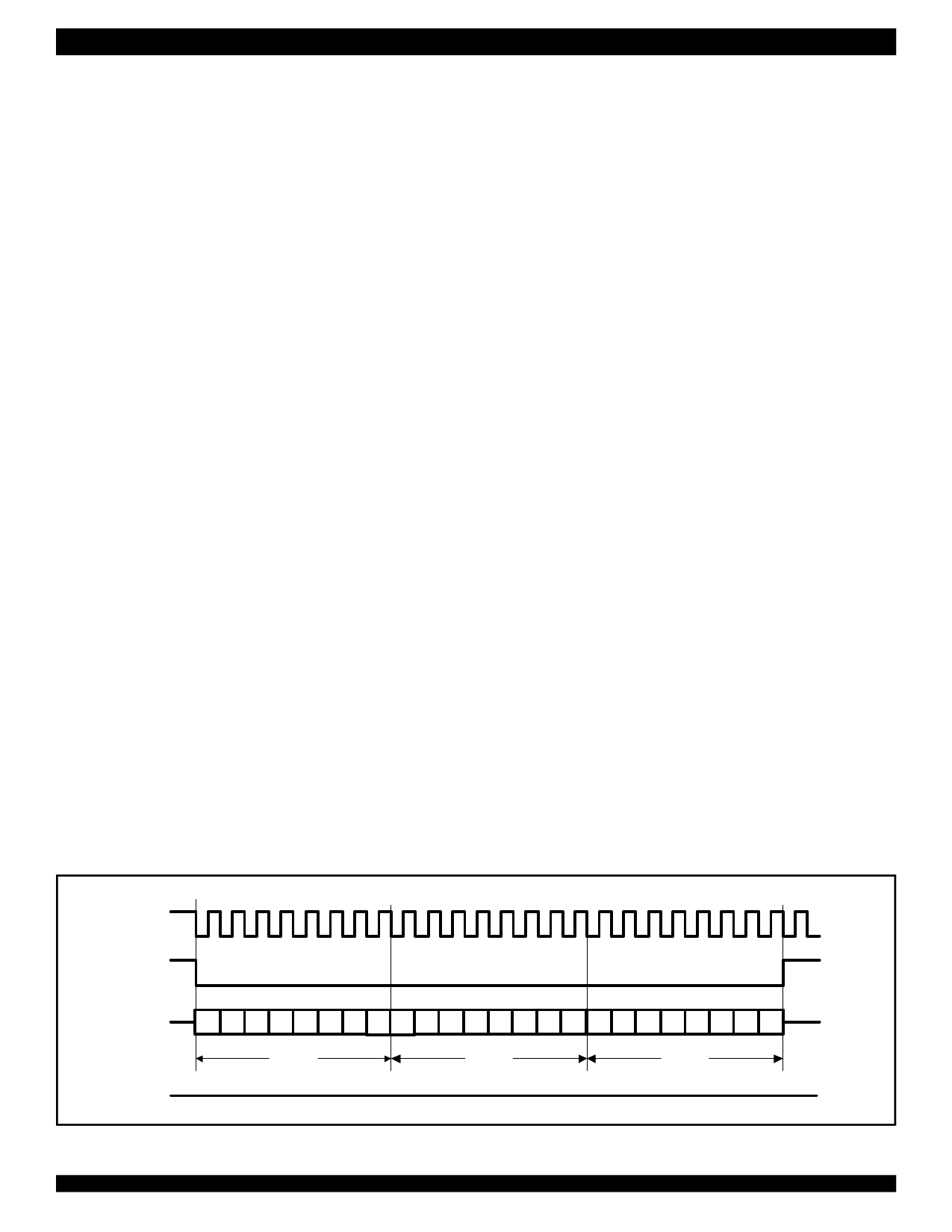
CCLK
CS
7654 321076 54321 0 76 54321 0
CI
Command
Data
Data
Byte
Byte 1
Byte 2
CO
High 'Z'
Figure 1. An Example of Serial Interface Write Mode
5
Share Link: 