IDT72V3612 Просмотр технического описания (PDF) - Integrated Device Technology
Номер в каталоге
Компоненты Описание
Список матч
IDT72V3612 Datasheet PDF : 25 Pages
| |||
IDT72V3612 3.3V, CMOS SyncBiFIFOTM
64 x 36 x 2
COMMERCIAL TEMPERATURE RANGE
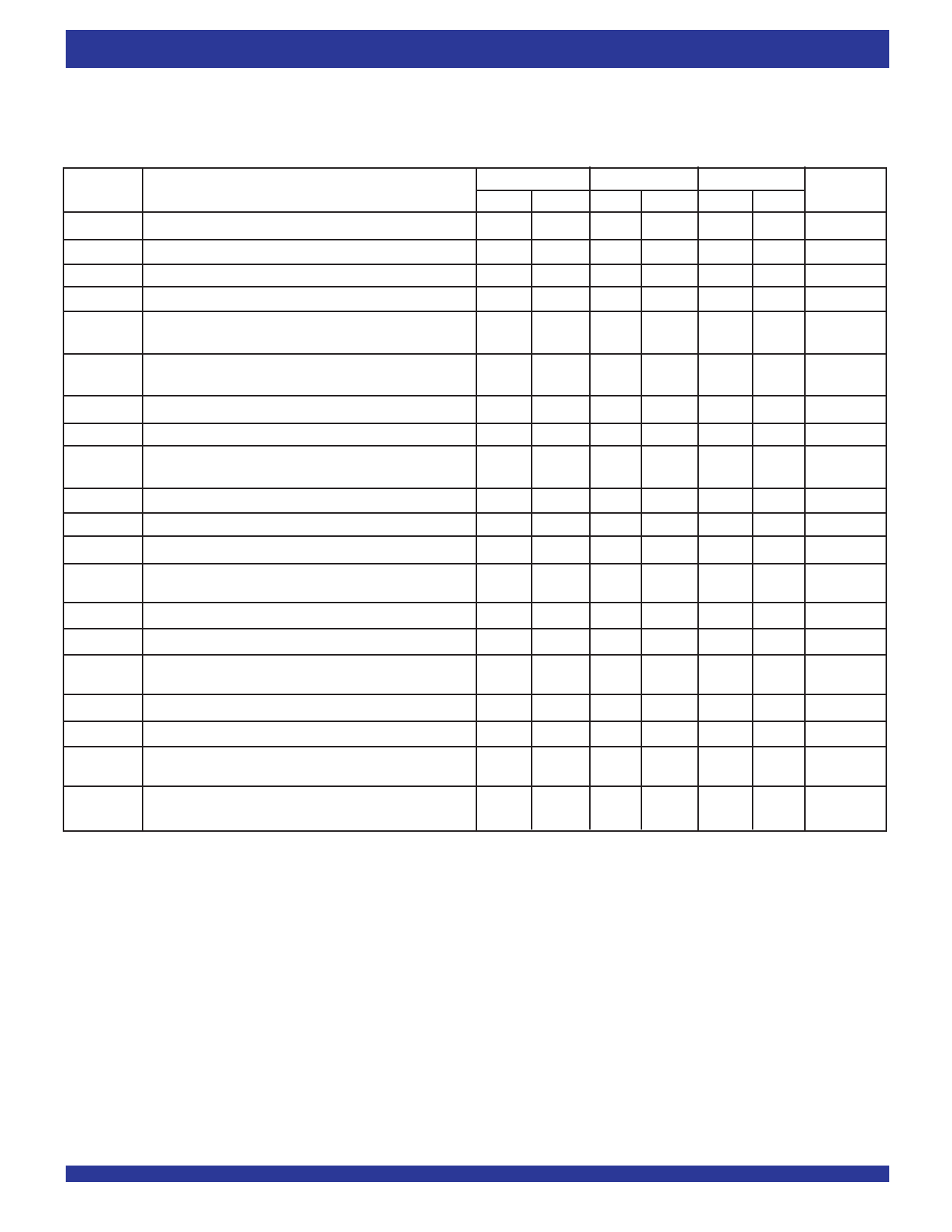
DC ELECTRICAL CHARACTERISTICS OVER RECOMMENDED RANGES OF
SUPPLY VOLTAGE AND OPERATING FREE-AIR TEMPERATURE
Commercial: Vcc=3.3V± 0.30V; for 12ns (83MHz) operation, Vcc=3.3V ±0.15V; TA = 0° C to +70°C; JEDEC JESD8-A compliant
Symbol
Parameter
IDT72V3612L12 IDT72V3612L15 IDT72V3612L20
Min. Max. Min. Max. Min. Max. Unit
fS
Clock Frequency, CLKA or CLKB
–
83
–
66.7
–
50
MHz
tCLK
Clock Cycle Time, CLKA or CLKB
12
–
15
–
20
–
ns
tCLKH
Pulse Duration, CLKA and CLKB HIGH
5
–
6
–
8
–
ns
tCLKL
Pulse Duration, CLKA and CLKB LOW
5
–
6
–
8
–
ns
tDS
Setup Time, A0-A35 before CLKA↑ and B0-B35 before
4
–
4
–
5
–
ns
CLKB↑
tENS1
Setup Time, CSA, W/RA before CLKA↑; CSB, W/RB
before CLKB↑
3.5
–
6
–
6
–
ns
tENS2
Setup Time, ENA, before CLKA↑; ENB before CLKB↑
3.5
–
4
–
5
–
ns
tENS3
Setup Time, MBA before CLKA↑: MBB before CLKB↑
3.5
–
4
–
5
–
ns
tPGS
Setup Time, ODD/EVEN and PGA before CLKA↑;
ODD/EVEN and PGB before CLKB↑(1)
3
–
4
–
5
–
ns
tRSTS
Setup Time, RST LOW before CLKA↑ or CLKB↑(2)
4
–
5
–
6
–
ns
tFSS
Setup Time, FS0/FS1 before RST HIGH
4
–
5
–
6
–
ns
tDH
Hold Time, A0-A35 after CLKA↑ and B0-B35 after CLKB↑ 0.5
–
1
–
1
–
ns
tENH1
Hold Time, CSA W/RA after CLKA↑; CSB, W/RB after
0.5
–
1
–
1
–
ns
CLKB↑
tENH2
Hold Time, ENA, after CLKA↑; ENB after CLKB↑
1
–
1
–
1
–
ns
tENH3
Hold Time, MBA after CLKA↑; MBB after CLKB↑
1
–
1
–
1
–
ns
tPGH
Hold Time, ODD/EVEN and PGA after CLKA↑;
ODD/EVEN and PGB after CLKB↑(1)
0
–
1
–
1
–
ns
tRSTH
Hold Time, RST LOW after CLKA↑ or CLKB↑(2)
4
–
5
–
6
–
ns
tFSH
Hold Time, FS0 and FS1 after RST HIGH
4
–
4
–
4
–
ns
tSKEW1(3) Skew Time, between CLKA↑ and CLKB↑ for EFA, EFB,
5.5
–
8
–
8
–
ns
FFA, and FFB
tSKEW2(3,4) Skew Time, between CLKA↑ and CLKB↑ for AEA, AEB,
14
–
14
–
16
–
ns
AFA, and AFB
NOTES:
1. Only applies for a clock edge that does a FIFO read.
2. Requirement to count the clock edge as one of at least four needed to reset a FIFO.
3. Skew time is not a timing constraint for proper device operation and is only included to illustrate the timing relationship between CLKA cycle and CLKB cycle.
4. Design simulated, not tested.
8
Share Link: 