71V016S15 Просмотр технического описания (PDF) - Integrated Device Technology
Номер в каталоге
Компоненты Описание
Список матч
71V016S15 Datasheet PDF : 9 Pages
| |||
IDT71V016, 3.3V CMOS Static RAM
1 Meg (64K x 16-Bit)
Commercial and Industrial Temperature Ranges
AC Electrical Characteristics (VDD = 3.3V ± 0.3V, Commercial and Industrial Temperature Ranges)
71V016S15
71V016S20
Symbol
Parameter
Min.
Max.
Min.
Max.
READ CYCLE
tRC
Read Cycle Time
15
____
20
___ _
tAA
Address Access Time
___ _
15
____
20
tACS
Chip Select Access Time
___ _
15
____
20
tCLZ(1)
Chip Select Low to Output in Low-Z
5
____
5
___ _
tCHZ(1)
Chip Select High to Output in High-Z
___ _
6
____
8
tOE
Output Enable Low to Output Valid
tOLZ(1)
Output Enable Low to Output in Low-Z
E tOHZ(1)
Output Enable High to Output in High-Z
tOH
Output Hold from Address Change
N C tBE
Byte Enable Low to Output Valid
I N tBLZ(1)
Byte Enable Low to Output in Low-Z
A tBHZ(1)
Byte Enable High to Output in High-Z
T E S S WRITE CYCLE
R C 16 N tWC
Write Cycle Time
A S 0 G tAW
Address Valid to End of Write
I tCW
Chip Select Low to End of Write
P E V S tBW
Byte Enable Low to End of Write
L 1 E tAS
Address Set-up Time
7 D tWR
Address Hold from End of Write
O R tWP
Write Pulse Width
S E W tDW
Data Valid to End of Write
D E tDH
Data Hold Time
B R N tOW(1)
Write Enable High to Output in Low-Z
tWHZ(1)
Write Enable Low to Output in High-Z
___ _
8
____
10
0
____
0
___ _
___ _
6
____
8
4
—
5
—
—
8
____
10
0
____
0
___ _
___ _
6
____
8
15
____
20
___ _
10
____
12
___ _
10
____
12
___ _
10
____
12
___ _
0
____
0
___ _
0
____
0
___ _
10
____
12
___ _
8
____
10
___ _
0
____
0
___ _
1
____
1
___ _
___ _
6
____
8
O O R NOTE:
FO 1. This parameter is guaranteed with the AC Load (Figure 2) by device characterization, but is not production tested.
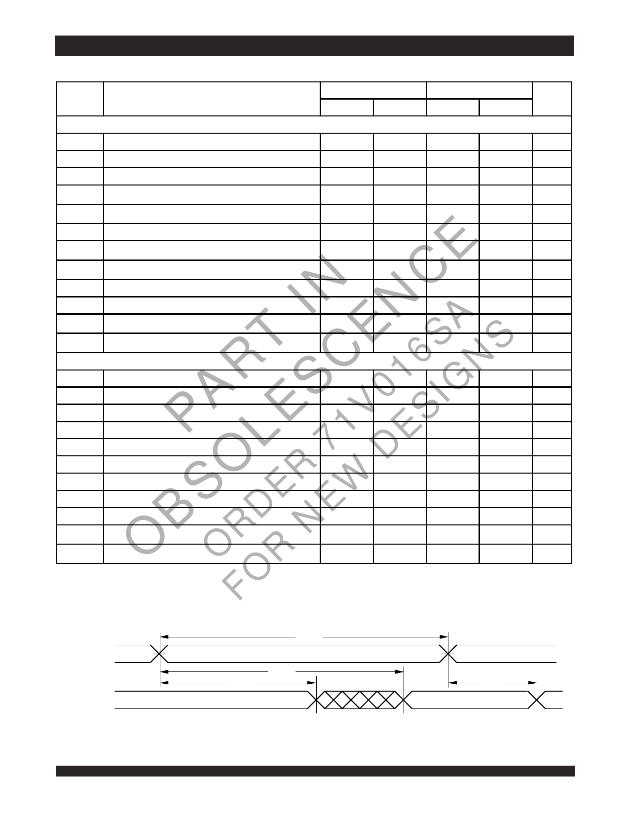
Timing Waveform of Read Cycle No. 1(1,2,3)
Unit
ns
ns
ns
ns
ns
ns
ns
ns
ns
ns
ns
ns
ns
ns
ns
ns
ns
ns
ns
ns
ns
ns
ns
3211 tbl 10
ADDRESS
DATAOUT
tRC
tAA
tOH
PREVIOUS DATAOUT VALID
tOH
DATAOUT VALID
NOTES:
1. WE is HIGH for Read Cycle.
2. Device is continuously selected, CS is LOW.
3. OE, BHE, and BLE are LOW.
6.452
3211 drw 07
Share Link: 