IDT71016S(2013) Просмотр технического описания (PDF) - Integrated Device Technology
Номер в каталоге
Компоненты Описание
Список матч
IDT71016S Datasheet PDF : 9 Pages
| |||
IDT71016, CMOS Static RAM
1 Meg (64K x 16-bit)
Commercial and Industrial Temperature Ranges
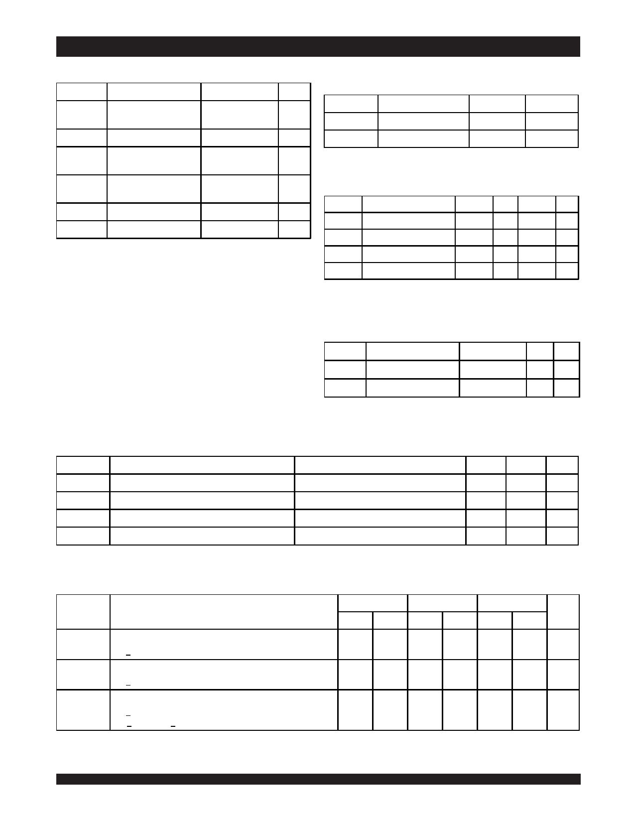
Absolute Maximum Ratings(1)
Symbol
Rating
Value
Unit
VTERM(2)
Terminal Voltage with
Respect to GND
-0.5 to +7.0
V
TBIAS
Temperature
Under Bias
-55 to +125
oC
TSTG
Storage
Temperature
-55 to +125
oC
PT
Power Dissipation
1.25
W
IOUT
DC Output Current
50
mA
NOTES:
3210 tbl 03
1. Stresses greater than those listed under ABSOLUTE MAXIMUM RATINGS may
cause permanent damage to the device. This is a stress rating only and functional
operation of the device at these or any other conditions above those indicated in the
operational sections of this specification is not implied. Exposure to absolute maximum
rating conditions for extended periods may affect reliability.
2. VTERM must not exceed VCC + 0.5V.
Recommended Operating
Temperature and Supply Voltage
Grade
Temperature
GND
VCC
Commercial
0°C to +70°C
0V
5.0V ± 10%
Industrial
–40°C to +85°C
0V
5.0V ± 10%
3210 tbl 04
Recommended DC Operating
Conditions
Symbol
Parameter
Min. Typ. Max. Unit
VCC Supply Voltage
4.5
5.0
5.5
V
GND Ground
0
0
0
V
VIH Input High Voltage
2.2
____ VDD +0.5 V
VIL Input Low Voltage
-0.5(1)
____
0.8
V
NOTE:
3210 tbl 05
1. VIL (min.) = –1.5V for pulse width less than tRC/2, once per cycle.
Capacitance
(TA = +25° C, f = 1.0MHz, SOJ/TSOP Package)
Symbol
Parameter(1)
Conditions Max. Unit
CIN Input Capacitance
VIN = 3dV
6 pF
CI/O I/O Capacitance
VOUT = 3dV
7 pF
NOTE:
3210 tbl 06
1. This parameter is guaranteed by device characterization, but not production
tested.
DC Electrical Characteristics
(VCC = 5.0V ± 10%, Commercial and Industrial Temperature Range)
Symbol
Parameter
Test Conditions
Min.
Max. Unit
|ILI|
Input Leakage Current
VCC = Max., VIN = GND to VCC
__ _
5
µA
|ILO|
Output Leakage Current
VCC = Max., CS = VIH, VOUT = GND to VCC
__ _
5
µA
VOL
Output Low Voltage
IOL = 8mA, VCC = Min.
__ _
0.4
V
VOH
Output High Voltage
IOH = -4mA, VCC = Min.
2.4
___
V
3210 tbl 07
DC Electrical Characteristics(1)
(VCC = 5.0V ± 10%, VLC = 0.2V, VHC = VCC–0.2V)
71016S12
71016S15
71016S20
Symbol
Parameter
Com'l. Com'l. Ind. Com'l. Ind. Unit
ICC
Dynamic Operating Current
CS < VIL, Outputs Open, VCC = Max., f = fMAX(2)
210
180
180
170
170
mA
ISB
Standby Power Supply Current (TTL Level)
CS > VIH, Outputs Open, VCC = Max., F = fMAX(2)
60
50
50
45
45
mA
Standby Power Supply Current (CMOS Level)
ISB1
CS > VHC, Outputs Open, VCC = Max., f = 0(2)
VIN < VLC or VIN > VHC
10
10
10
10
10
mA
NOTES:
1. All values are maximum guaranteed values.
2. fMAX = 1/tRC (all address inputs are cycling at fMAX); f = 0 means no address input lines are changing .
3210 tbl 08
6.432
Share Link: 