8405202QA Просмотр технического описания (PDF) - Intersil
Номер в каталоге
Компоненты Описание
Список матч
8405202QA Datasheet PDF : 37 Pages
| |||
80C86
Minimum Mode System (Continued)
The following pin function descriptions are for the 80C86 in minimum mode (i.e., MN/MX = VCC). Only the pin functions which are unique to minimum
mode are described; all other pin functions are as described in the following.
SYMBOL
PIN
NUMBER
TYPE
DESCRIPTION
HOLD
HLDA
31, 30
I
HOLD: indicates that another master is requesting a local bus “hold”. To be an acknowledged, HOLD
O
must be active HIGH. The processor receiving the “hold” will issue a “hold acknowledge” (HLDA) in
the middle of a t4 or TI clock cycle. Simultaneously with the issuance of HLDA, the processor will float
the local bus and control lines. After HOLD is detected as being LOW, the processor will lower HLDA,
and when the processor needs to run another cycle, it will again drive the local bus and control lines.
HOLD is not an asynchronous input. External synchronization should be provided if the system cannot
otherwise guarantee the setup time.
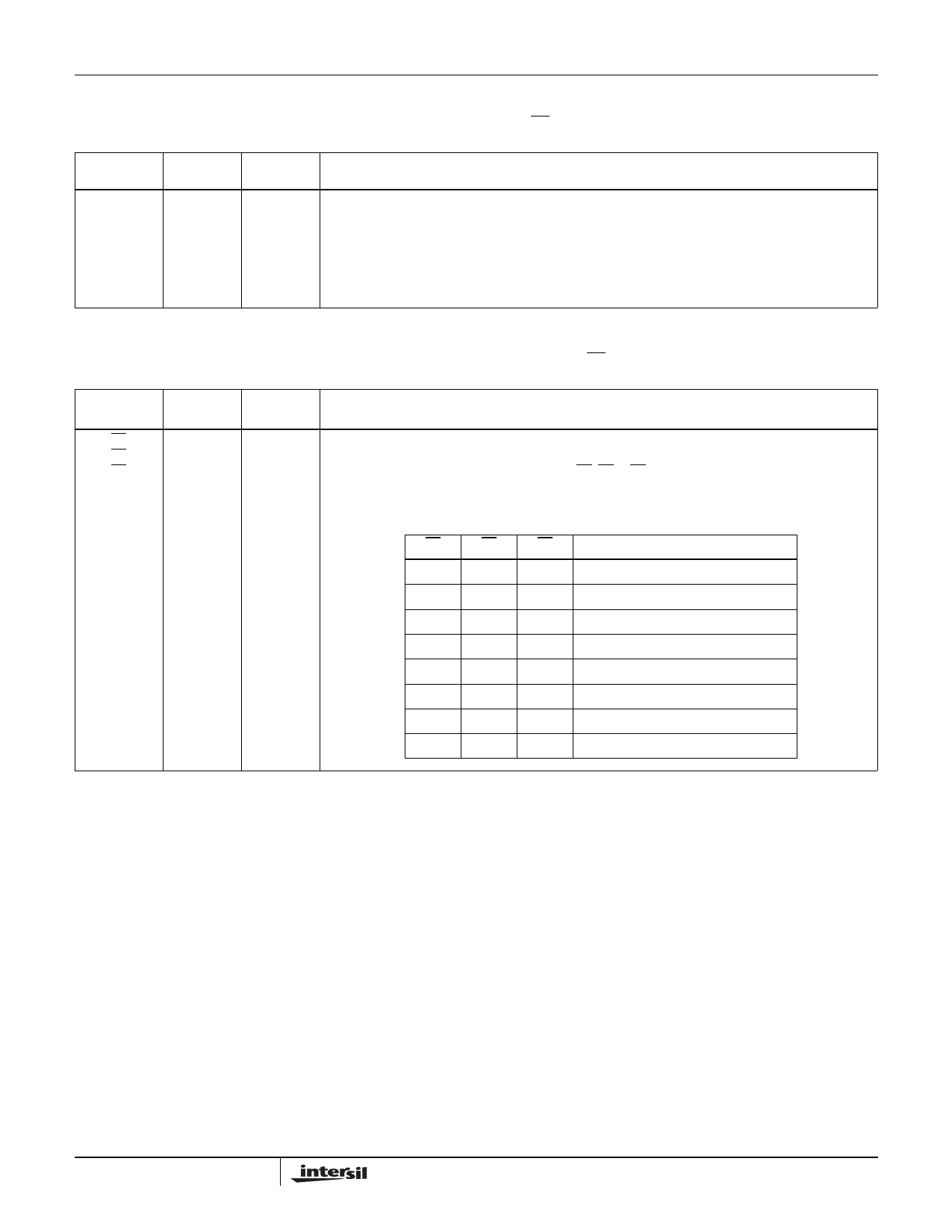
Maximum Mode System
The following pin function descriptions are for the 80C86 system in maximum mode (i.e., MN/MX - GND). Only the pin functions which are unique
to maximum mode are described in the following.
SYMBOL
PIN
NUMBER
TYPE
DESCRIPTION
S0
26
O
STATUS: is active during t4, t1 and t2 and is returned to the passive state (1, 1, 1) during t3 or during
S1
27
O
tW when READY is HIGH. This status is used by the 82C88 Bus Controller to generate all memory
S2
28
O
and I/O access control signals. Any change by S2, S1 or S0 during t4 is used to indicate the beginning
of a bus cycle, and the return to the passive state in t3 or tW is used to indicate the end of a bus cycle.
These signals are held at a high impedance logic one state during “grant sequence”.
S2
S1
S0
CHARACTERISTICS
0
0
0 Interrupt Acknowledge
0
0
1 Read I/O Port
0
1
0 Write I/O Port
0
1
1 Halt
1
0
0 Code Access
1
0
1 Read Memory
1
1
0 Write Memory
1
1
1 Passive
6
FN2957.3
January 9, 2009
Share Link: 