8405202QA Просмотр технического описания (PDF) - Intersil
Номер в каталоге
Компоненты Описание
Список матч
8405202QA Datasheet PDF : 37 Pages
| |||
80C86
Pin Descriptions
The following pin function descriptions are for 80C86 systems in either minimum or maximum mode. The “Local Bus” in these description is the direct
multiplexed bus interface connection to the 80C86 (without regard to additional bus buffers).
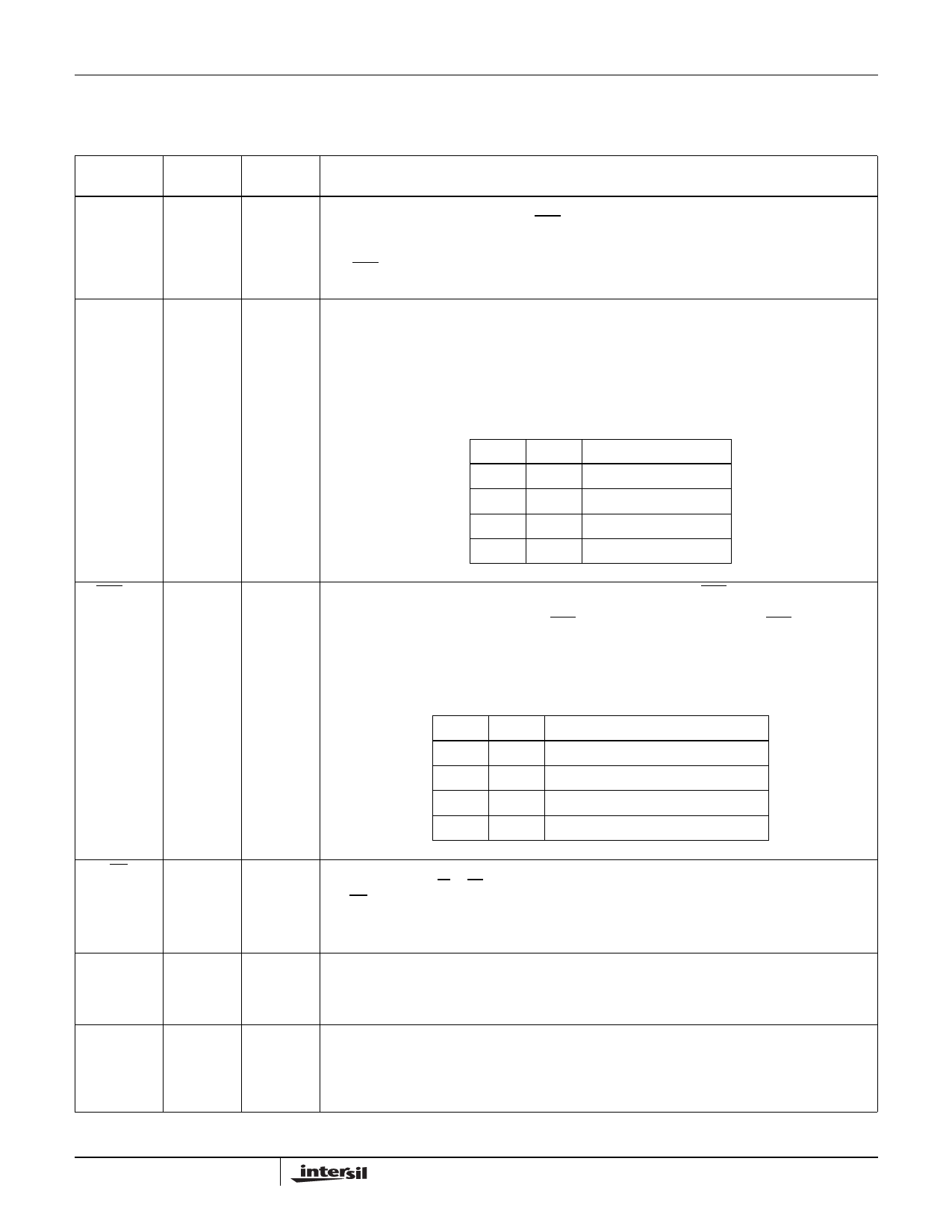
SYMBOL
PIN
NUMBER
TYPE
DESCRIPTION
AD15-AD0 2-16, 39
I/O
ADDRESS DATA BUS: These lines constitute the time multiplexed memory/lO address (t1) and data
(t2, t3, tW, t4) bus. A0 is analogous to BHE for the lower byte of the data bus, pins D7-D0. It is LOW
during Ti when a byte is to be transferred on the lower portion of the bus in memory or I/O operations.
Eight-bit oriented devices tied to the lower half would normally use A0 to condition chip select functions
(See BHE). These lines are active HIGH and are held at high impedance to the last valid logic level
during interrupt acknowledge and local bus “hold acknowledge” or “grant sequence”.
A19/S6
A18/S5
A17/S4
A16/S3
35-38
O
ADDRESS/STATUS: During t1, these are the 4 most significant address lines for memory operations.
During I/O operations these lines are LOW. During memory and I/O operations, status information is
available on these lines during t2, t3, tW, t4. S6 is always LOW. The status of the interrupt enable
FLAG bit (S5) is updated at the beginning of each clock cycle. S4 and S3 are encoded as shown.
This information indicates which segment register is presently being used for data accessing.
These lines are held at high impedance to the last valid logic level during local bus “hold acknowledge”
or “grant sequence”.
S4
S3
CHARACTERISTICS
0
0 Alternate Data
0
1 Stack
1
0 Code or None
1
1 Data
BHE/S7
34
O
BUS HIGH ENABLE/STATUS: During t1 the bus high enable signal (BHE) should be used to enable
data onto the most significant half of the data bus, pins D15-D8. Eight bit oriented devices tied to the
upper half of the bus would normally use BHE to condition chip select functions. BHE is LOW during
t1 for read, write, and interrupt acknowledge cycles when a byte is to be transferred on the high portion
of the bus. The S7 status information is available during t2, t3 and t4. The signal is active LOW, and
is held at high impedance to the last valid logic level during interrupt acknowledge and local bus “hold
acknowledge” or “grant sequence”, it is LOW during t1 for the first interrupt acknowledge cycle.
BHE
0
0
1
1
A0
CHARACTERISTICS
0 Whole Word
1 Upper Byte From/to Odd Address
0 Lower Byte From/to Even address
1 None
RD
32
READY
22
INTR
18
O
READ: Read strobe indicates that the processor is performing a memory or I/O read cycle, depending
on the state of the M/IO or S2 pin. This signal is used to read devices which reside on the 80C86 local
bus. RD is active LOW during t2, t3 and tW of any read cycle, and is guaranteed to remain HIGH in t2
until the 80C86 local bus has floated.
This line is held at a high impedance logic one state during “hold acknowledge” or “grand sequence”.
I
READY: The acknowledgment from the addressed memory or I/O device that will complete the data
transfer. The RDY signal from memory or I/O is synchronized by the 82C84A Clock Generator to form
READY. This signal is active HIGH. The 80C86 READY input is not synchronized. Correct operation
is not guaranteed if the Setup and Hold Times are not met.
I
INTERRUPT REQUEST: A level triggered input which is sampled during the last clock cycle of each
instruction to determine if the processor should enter into an interrupt acknowledge operation. A
subroutine is vectored to via an interrupt vector lookup table located in system memory. It can be
internally masked by software resetting the interrupt enable bit.
lNTR is internally synchronized. This signal is active HIGH.
4
FN2957.3
January 9, 2009
Share Link: 