ICS94206F-T Просмотр технического описания (PDF) - Integrated Circuit Systems
Номер в каталоге
Компоненты Описание
Список матч
ICS94206F-T Datasheet PDF : 18 Pages
| |||
ICS94206
General Description
The ICS94206 is a single chip clock solution for desktop designs using the BX/Apollo Pro133/ALI 1631 style chipset. It provides all
necessary clock signals for such a system.
The ICS94206 belongs to ICS new generation of programmable system clock generators. It employs serial programming I2C
interface as a vehicle for changing output functions, changing output frequency, configuring output strength, configuring output to
output skew, changing spread spectrum amount, changing group divider ratio and dis/enabling individual clocks. This device also
has ICS propriety 'Watchdog Timer' technology which will reset the frequency to a safe setting if the system become unstable from
over clocking.
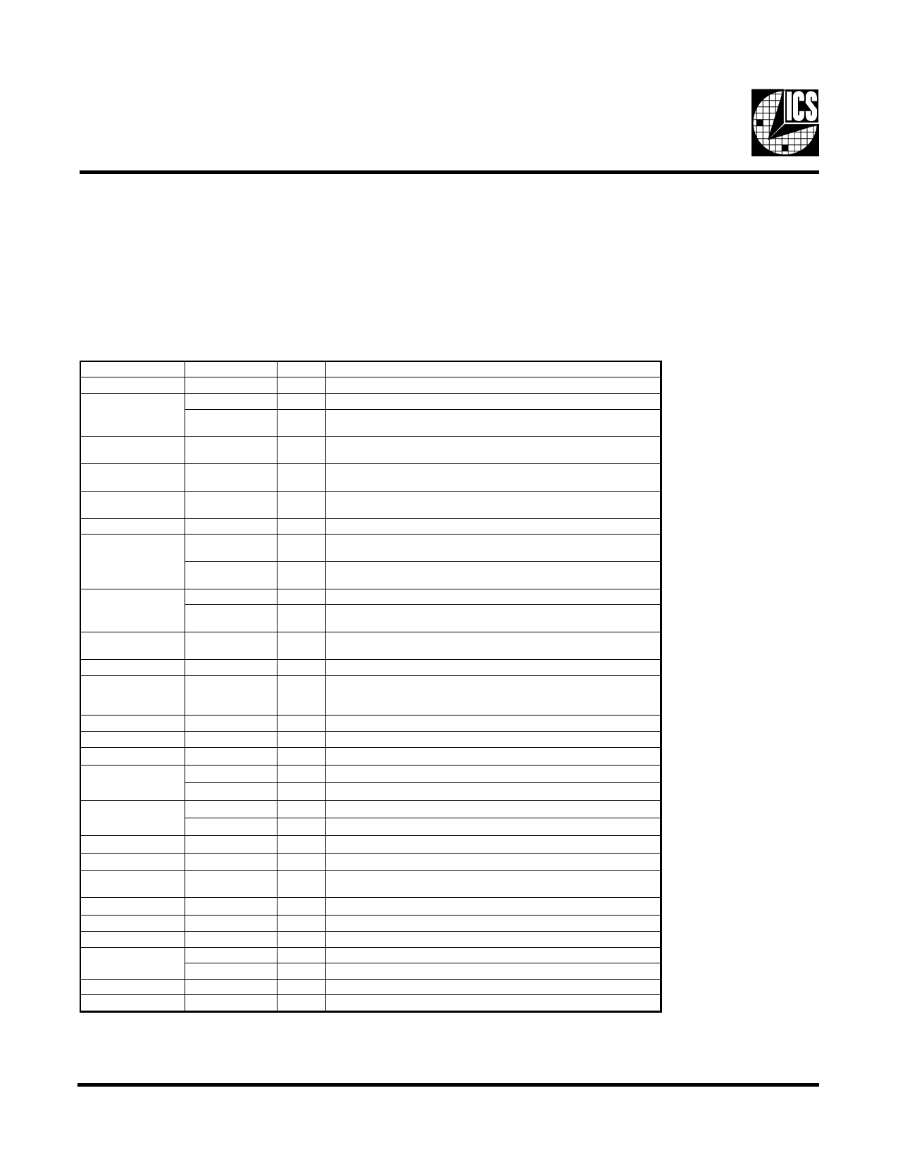
Pin Configuration
PIN NUMBER
1
2
3,9,16,22,
33,39,45
4
PIN NAME
VDD1
REF0
PCI_STOP#1
GND
X1
5
X2
6,14
VDD2
PCICLK_F
7
MODE1, 2
FS3
8
PCICLK0
13, 12, 11, 10
15
17, 18, 20, 21,
28, 29, 31, 32,
34, 35,37,38
19,30,36
23
24
25
26
27
40
41
42
43
44
46
47
48
PCICLK(4:1)
BUFFER IN
SDRAM (11:0)
VDD3
SDATA
SCLK
24MHz
FS11, 2
48MHz
FS01, 2
VDD4
SDRAM_F
CLK_STOP#
VDDL2
CPUCLK1
CPUCLK_F
REF1
FS21, 2
IOAPIC
VDDL1
TYPE
PWR
OUT
IN
DESCRIPTION
Ref, XTAL power supply, nominal 3.3V
14.318 Mhz reference clock.
Halts PCICLK clocks at logic 0 level, when input low (In mobile
mode, MODE=0)
PWR Ground
IN
OUT
PWR
OUT
IN
IN
OUT
OUT
IN
Crystal input, has internal load cap (36pF) and feedback
resistor from X2
Crystal output, nominally 14.318MHz. Has internal load
cap (36pF)
Supply for PCICLK_F and PCICLK (0:4), nominal 3.3V
Free running PCI clock not affected by PCI_STOP# for power
management.
Pin 7 function select pin, 1=Desktop Mode, 0=Mobile Mode.
Latched Input.
Frequency select pin. Latched Input. Internal Pull-down to GND
PCI clock outputs. Syncheronous to CPU clocks with 1-48ns skew
(CPU early)
PCI clock outputs. Syncheronous to CPU clocks with 1-48ns skew
(CPU early)
Input to Fanout Buffers for SDRAM outputs.
OUT
SDRAM clock outputs, Fanout Buffer outputs from BUFFER IN pin
(controlled by chipset).
PWR
I/O
IN
OUT
IN
OUT
IN
PWR
OUT
IN
PWR
OUT
OUT
OUT
IN
OUT
PWR
Supply for SDRAM (0:12) and CPU PLL Core, nominal 3.3V.
Data pin for I2C circuitry 5V tolerant
Clock input of I2C input, 5V tolerant input
24MHz output clock
Frequency select pin. Latched Input.
48MHz output clock
Frequency select pin. Latched Input
Power for 24 & 48MHz output buffers and fixed PLL core.
Free running SDRAM clock output. Not affected by CPU_STOP#
This asynchronous input halts CPUCLK1, IOAPIC & SDRAM
(0:11) at logic "0" level when driven low.
Supply for CPU clocks, either 2.5V or 3.3V nominal
CPU clock outputs, powered by VDDL2. Low if CPU_STOP#=Low
Free running CPU clock. Not affected by the CPU_STOP#
14.318 MHz reference clock.
Frequency select pin. Latched Input
IOAPIC clock output. 14.318 MHz Powered by VDDL1.
Supply for IOAPIC, either 2.5 or 3.3V nominal
Notes:
1: Internal Pull-up Resistor of 120K to 3.3V on indicated inputs
2: Bidirectional input/output pins, input logic levels are latched at internal power-on-reset. Use 10Kohm resistor
to program logic Hi to VDD or GND for logic low.
2
Share Link: 