HMC707LP5 Просмотр технического описания (PDF) - Hittite Microwave
Номер в каталоге
Компоненты Описание
Список матч
HMC707LP5 Datasheet PDF : 12 Pages
| |||
HMC707LP5 / 707LP5E
v04.0409
0.5 dB LSB 6-BIT DIGITAL
VARIABLE GAIN AMPLIFIER, 700 - 1200 MHz
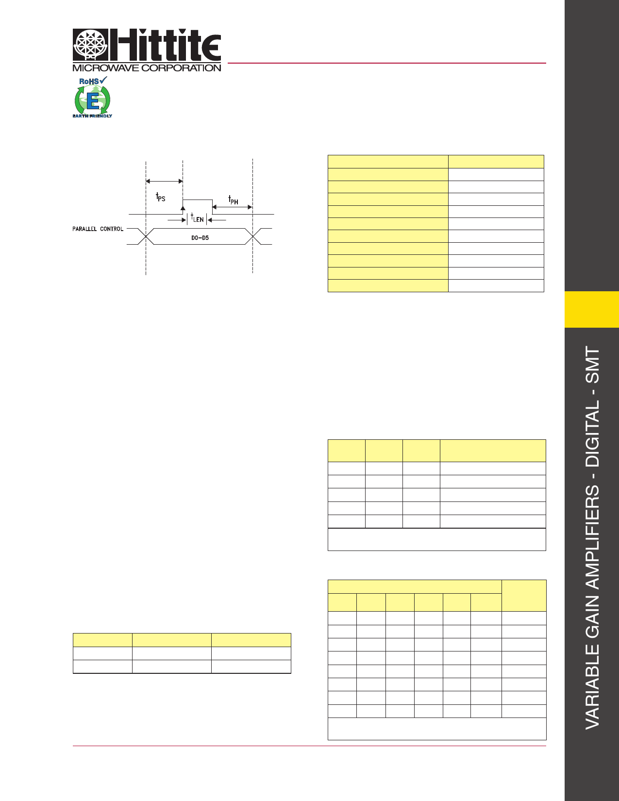
Timing Diagram (Latched Parallel Mode)
Parameter
Typ.
Min. serial period, tSCK
Control set-up time, tCS
Control hold-time, tCH
LE setup-time, tLN
Min. LE pulse width, tLEW
Min LE pulse spacing, tLES
Serial clock hold-time from LE, tCKN
Hold Time, tPH
Latch Enable Minimum Width, tLEN
Setup Time, tPS
100 ns
20 ns
20 ns
10 ns
10 ns
630 ns
10 ns
0 ns
10 ns
2 ns
Parallel Mode (Direct Parallel Mode & Latched Parallel Mode)
Note: The parallel mode is enabled when P/S is set to low.
Direct Parallel Mode - The attenuation state is changed by the Control Voltage Inputs directly. The LE (Latch Enable)
must be at a logic high to control the attenuator in this manner.
Latched Parallel Mode - The attenuation state is selected using the Control Voltage Inputs and set while the LE is in
the Low state. The attenuator will not change state while LE is Low. Once all Control Voltage Inputs are at the desired
states the LE is pulsed. See timing diagram above for reference.
Power-Up States
If LE is set to logic LOW at power-up, the logic state of
PUP1 and PUP2 determines the power-up state of the
part per PUP truth table. If the LE is set to logic HIGH
at power-up, the logic state of D0-D5 determines the
power-up state of the part per truth table. The DVGA
latches in the desired power-up state approximately
200 ms after power-up.
Power-On Sequence
The ideal power-up sequence is: GND, Vdd, digital
inputs, RF inputs. The relative order of the digital
inputs are not important as long as they are powered
after Vdd / GND
Control Voltage Table
State
Low
High
Vdd = +3V
0 to 0.5V @ <1 µA
2 to 3V @ <1 µA
Vdd = +5V
0 to 0.8V @ <1 µA
2 to 5V @ <1 µA
PUP Truth Table
LE
PUP1
PUP2
Gain Relative to Maximum
Gain
0
0
0
-31.5
0
1
0
-24
0
0
1
-16
0
1
1
Insertion Loss
1
X
X
0 to -31.5 dB
Note: Power-Up with LE= 1 provides normal parallel operation
with D0 - D5, and PUP1 and PUP2 are not active.
Truth Table
Control Voltage Input
Reference
Insertion
D5
D4
D3
D2
D1
D0
Loss
High High High High High High
0 dB
High High High High High Low
-0.5 dB
High High High High Low High
-1 dB
High High High Low High High
-2 dB
High High Low High High High
-4 dB
High Low High High High High
-8 dB
Low High High High High High
-16 dB
Low Low Low Low Low Low -31.5 dB
Any combination of the above states will provide an attenuation
equal to the sum of the bits selected.
For price, delivery and to place orders: Hittite Microwave Corporation, 20 Alpha Road, Chelmsford, MA 01824
Phone: 978-250-3343 Fax: 978-250-3373 Order On-line at www.hittite.com
Application Support: Phone: 978-250-3343 or apps@hittite.com
12
12 - 6
Share Link: 