HMC707LP5 Просмотр технического описания (PDF) - Hittite Microwave
Номер в каталоге
Компоненты Описание
Список матч
HMC707LP5 Datasheet PDF : 12 Pages
| |||
HMC707LP5 / 707LP5E
v04.0409
0.5 dB LSB 6-BIT DIGITAL
VARIABLE GAIN AMPLIFIER, 700 - 1200 MHz
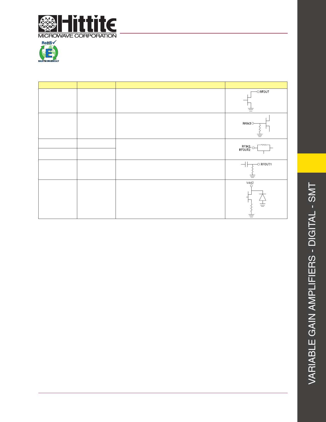
Pin Descriptions (Continued)
Pin Number
Function
Description
20
RFOUT
RF Output and DC BIAS for the second amplifier (AMP2).
See Application Circuit for off-chip components.
22
RFIN3
RF input for the second amplifier (AMP2). This pin is DC
coupled. An off-chip DC blocking capacitor is required.
27
RFIN2
Input and output of the 6-bit digital attenuator (6-Bit DAT).
These pins are DC coupled and matched to 50 Ohms.
24
RFOUT2
Blocking capacitors are required. Select value based
on lowest frequency of operation.
29
RFOUT1
RF output for the first amplifier (AMP1).
This pin is matched to 50 Ohms.
Interface Schematic
12
31
Vdd2
Power Supply Voltage for the first amplifier. Choke inductor
and bypass capacitors are required. See application circuit.
For price, delivery and to place orders: Hittite Microwave Corporation, 20 Alpha Road, Chelmsford, MA 01824
Phone: 978-250-3343 Fax: 978-250-3373 Order On-line at www.hittite.com
Application Support: Phone: 978-250-3343 or apps@hittite.com
12 - 10
Share Link: 