HIP6020A Просмотр технического описания (PDF) - Intersil
Номер в каталоге
Компоненты Описание
Список матч
HIP6020A Datasheet PDF : 16 Pages
| |||
HIP6020A
Absolute Maximum Ratings
Supply Voltage, VCC . . . . . . . . . . . . . . . . . . . . . . . . . . . . . . . . .+15V
PGOOD, RT/FAULT, DRIVE, PHASE, and
GATE Voltage . . . . . . . . . . . . . . . . . . . GND - 0.3V to VCC + 0.3V
Input, Output or I/O Voltage . . . . . . . . . . . . . . . . . . GND -0.3V to 7V
ESD Classification . . . . . . . . . . . . . . . . . . . . . . . . . . . . . . . . Class 1
Recommended Operating Conditions
Supply Voltage, VCC . . . . . .
Ambient Temperature Range
.
.
.
.
.
.
.
.
.
.
.
.
.
.
.
.
.
.
.
.
.
.
.
.
.
.
.
.
.
.
.
.
.
.
.
.
.
.
.
.
.
+12V ±10%
0oC to 70oC
Junction Temperature Range. . . . . . . . . . . . . . . . . . . 0oC to 125oC
Thermal Information
Thermal Resistance (Typical, Note 1)
θJA (oC/W)
SOIC Package . . . . . . . . . . . . . . . . . . . . . . . . . . . .
70
Maximum Junction Temperature (Plastic Package) . . . . . . . . 150oC
Maximum Storage Temperature Range . . . . . . . . . . -65oC to 150oC
Maximum Lead Temperature (Soldering 10s) . . . . . . . . . . . . . 300oC
(SOIC - Lead Tips Only)
CAUTION: Stresses above those listed in “Absolute Maximum Ratings” may cause permanent damage to the device. This is a stress only rating and operation of the
device at these or any other conditions above those indicated in the operational sections of this specification is not implied.
NOTE:
1. θJA is measured with the component mounted on a low effective thermal conductivity test board in free air. See Tech Brief TB379 for details.
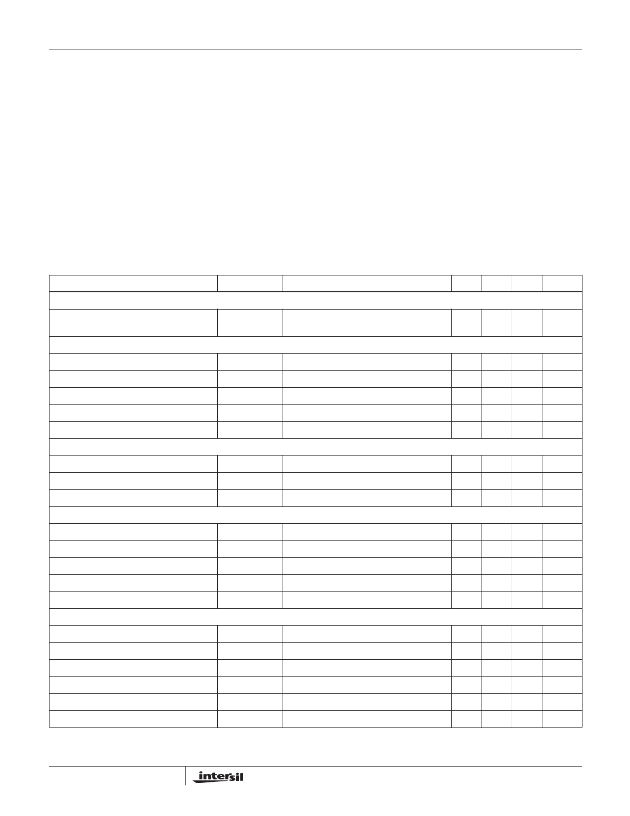
Electrical Specifications Recommended Operating Conditions, Unless Otherwise Noted. Refer to Figures 1, 2 and 3
PARAMETER
SYMBOL
TEST CONDITIONS
MIN TYP MAX
VCC SUPPLY CURRENT
Nominal Supply Current
ICC
UGATE1, LGATE1, UGATE2, DRIVE3, and -
9
-
DRIVE4 Open
POWER-ON RESET
Rising VCC Threshold
Falling VCC Threshold
Rising VAUX Threshold
VAUX Threshold Hysteresis
Rising VOCSET1 Threshold
OSCILLATOR
VOCSET = 4.5V
VOCSET = 4.5V
VOCSET = 4.5V
VOCSET = 4.5V
-
- 10.4
8.2
-
-
-
2.5
-
-
0.5
-
-
1.26
-
Free Running Frequency
Total Variation
FOSC
RT = OPEN
6kΩ < RT to GND < 200kΩ
185 200 215
-15
-
+15
Ramp Amplitude
∆VOSC
DAC AND STANDARD BUCK REGULATOR REFERENCE
RT = Open
-
1.9
-
DAC(VID0-VID4) Input Low Voltage
0.8
DAC(VID0-VID4) Input High Voltage
2.0
DACOUT Voltage Accuracy
-1.0
-
+1.0
PWM2 Reference Voltage
SELECT < 0.8V
-
1.5
-
PWM2 Reference Voltage Tolerance
-
3
-
LINEAR REGULATORS (VOUT3 AND VOUT4)
Regulation
-
3
-
FB3 Regulation Voltage
FB4 Regulation Voltage
FB3,4 Under-Voltage Level
FB3,4 Under-Voltage Hysteresis
VREG3
VREG4
FBUV
FB Rising
-
1.5
-
-
1.8
-
-
75
-
7
Output Drive Current
VAUX-VDRIVE > 0.6V
20 40
-
UNITS
mA
V
V
V
V
V
kHz
%
VP-P
V
V
%
V
%
%
V
V
%
%
mA
4
Share Link: 