FM25V01 Просмотр технического описания (PDF) - Cypress Semiconductor
Номер в каталоге
Компоненты Описание
Список матч
FM25V01 Datasheet PDF : 18 Pages
| |||
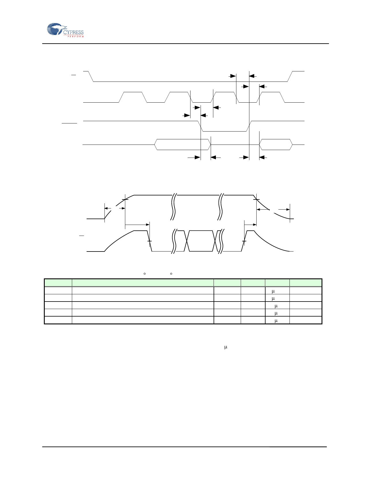
/HOLD Timing
S
C
tHS
HOLD
Q
Power Cycle Timing
VDD
S
VDD min.
tVR
tPU
FM25V01 - 128Kb SPI FRAM
tHS
tHH
tHH
tHZ
tLZ
tVF
tPD
Power Cycle & Sleep Timing (TA = -40 C to + 85 C, VDD = 2.0V to 3.6V, unless otherwise specified)
Symbol Parameter
Min Max Units Notes
tVR
VDD Rise Time
tVF
VDD Fall Time
tPU
Power Up (VDD min) to First Access (/S low)
tPD
Last Access (/S high) to Power Down (VDD min)
tREC
Recovery Time from Sleep Mode
50
-
s/V
1,2
100
-
s/V
1,2
250
-
s
3
0
-
s
-
400
s
Notes
1. This parameter is characterized and not 100% tested.
2. Slope measured at any point on VDD waveform.
3. Applies to VDD > 2.7V. When powering up to VDD < 2.7V, the tPU limit is 500 s.
Document Number: 001-84492 Rev. *B
Page 13 of 18
Share Link: 