FM24C64B Просмотр технического описания (PDF) - Cypress Semiconductor
Номер в каталоге
Компоненты Описание
Список матч
FM24C64B Datasheet PDF : 15 Pages
| |||
AC Test Conditions
Input Pulse Levels
Input rise and fall times
Input and output timing levels
0.1 VDD to 0.9 VDD
10 ns
0.5 VDD
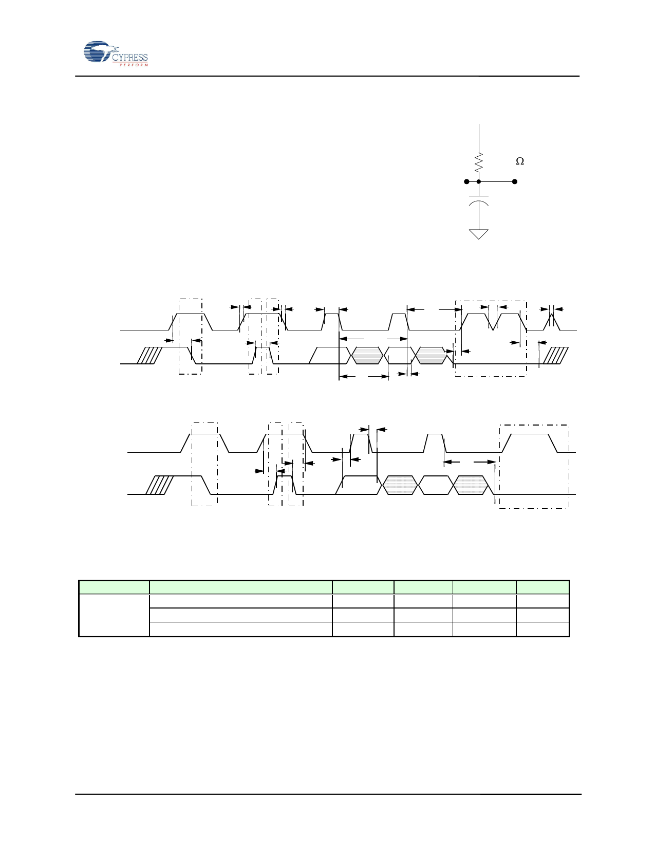
Diagram Notes
All start and stop timing parameters apply to both read and write
cycles. Clock specifications are identical for read and write cycles.
Write timing parameters apply to slave address, word address, and
write data bits. Functional relationships are illustrated in the relevant
data sheet sections. These diagrams illustrate the timing parameters
only.
FM24C64B
Equivalent AC Load Circuit
5.5V
Output
1700
100 pF
Read Bus Timing
tR
t HIGH
tF
t LOW
t SP
t SP
SCL
SDA
t SU:SDA
t BUF
1/fSCL
t HD:DAT
t SU:DAT
Start
Stop Start
t AA
t DH
Acknowledge
Write Bus Timing
SCL
SDA
t SU:STO
t HD:STA
t HD:DAT
t SU:DAT
Start
Stop Start
t AA
Acknowledge
Data Retention
Symbol
Parameter
TDR
@ +85ºC
@ +80ºC
@ +75ºC
Min
Max
Units
Notes
10
-
Years
19
-
Years
38
-
Years
Document Number: 001-84454 Rev. *B
Page 10 of 15
Share Link: 