FAN7313 Просмотр технического описания (PDF) - Fairchild Semiconductor
Номер в каталоге
Компоненты Описание
Список матч
FAN7313 Datasheet PDF : 11 Pages
| |||
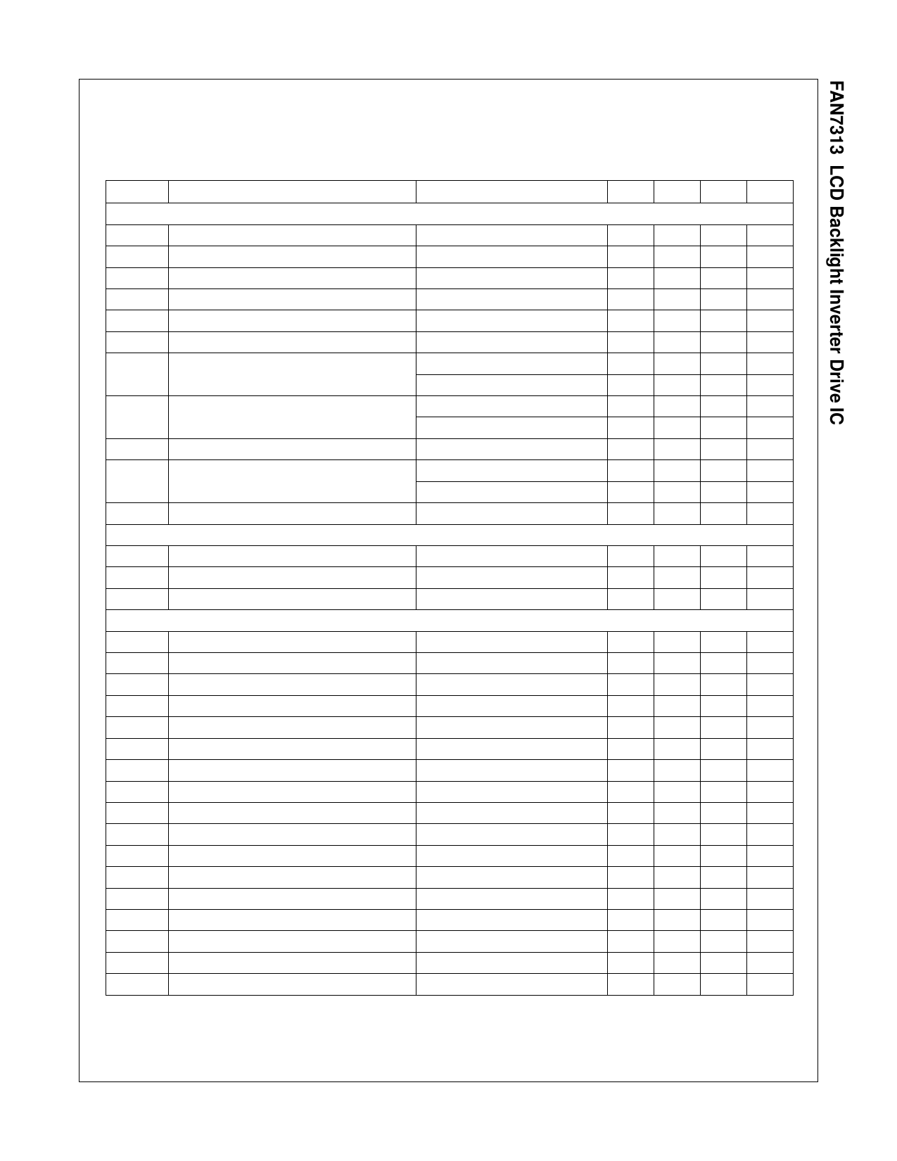
Electrical Characteristics (Continued)
For typical values TA=25°C and VIN=18V. For min./max. values, TA is the operating ambient temperature range with
-25°C ≤ TA ≤ 85°C and 4.5V ≤ VIN ≤ 18V, unless otherwise specified. Specifications to -25°C ~ 85°C are guaranteed by
design based on final characterization results.
Symbol Characteristics
Test Condition
Min. Typ. Max. Unit
PROTECTION SECTION
Vscp
Vcmpr
Volp
Vovp
Volr
Volrhy
Short-Circuit Protection Voltage
CMP Protection Voltage
Open-Lamp Protection Voltage
Over-Voltage Protection
Open-Lamp Regulation Voltage
Opem-Lamp Regulation Hystersis(5)
Tscp Short-Circuit Protection Delay
Tcmp
Tolp
Tolr
CMP Protection Delay
Open-Lamp Protection Delay
Open-Lamp Regulation Delay
FB=OLP=2V
Striking, Foscb=300Hz
Normal, Fosc=100kHz
Striking, Foscb=300Hz
Normal Fosc=100kHz
Foscb=300Hz
Striking, OLR=2.5V
Normal, OLR=2.5V
1.9 2.0 2.1 V
2.1 2.3 2.5 V
0.95 1.00 1.08 V
2.85 3.00 3.15 V
1.9 2.0 2.1 V
250
mV
1.7 2.0 2.3 µsec
100 300 500 µsec
1.7 2.0 2.3 sec
100 300 500 µsec
1.7 2.0 2.3 sec
1.7 2.0 2.3 sec
100 300 500 µsec
TSD Thermal Shutdown
150
°C
ENABLE SECTION
Vena Enable State Input Voltage
Vdis Disable State Input Voltage
Iena Enable Discharge Current
OUTPUT SECTION
fnrmo
fstro
Output Normal Frequency(6)
Output Striking Frequency(6)
VFB=1V, RT=27kΩ
VFB=0V, RT=27kΩ
Vuvh High-Side Output Voltage Before Start-up
Vuvl Low-Side Output Voltage Before Start-up
Venh High-Side Output Voltage at Vena=0V
Venl Low-Side Output Voltage at Vena=0V
OUTH High-Side Output Voltage
2
5
V
0.7 V
0.2 1.0 4.0 µA
48 50 52 KHz
62 65 68 KHz
-0.5
0.5 V
-0.5
0.5 V
-0.5
0.5 V
-0.5
0.5 V
5.5 6.0 6.5 V
OUTL Low-Side Output Voltage
Idsurh
Idsinh
Idsurl
Idsinl
trh
tfh
trl
tfl
High-Side Output Drive Soure Current(5)
High-Side Output Drive Sink Current(5)
Low-Side Output Drive Soure Current(5)
Low-Side Output Drive Sink Current(5)
High-Side Output Rising Time(5)
High-Side Output Falling Time(5)
Low-Side Output Rising Time(5)
Low-Side Output Falling Time(5)
VIN=18V
VIN=18V
VIN=18V
VIN=18V
VIN=18V, Cload=4.7nF
VIN=18V, Cload=4.7nF
VIN=18V, Cload=4.7nF
VIN=18V, Cload=4.7nF
tdead Dead Time
Notes:
5. These parameters, although guaranteed, are not 100% tesed in production.
6. Output frequency is half fosc.
5.5 6.0 6.5 V
530
mA
530
mA
530
mA
530
mA
100
nsec
100
nsec
100
nsec
100
nsec
430
nsec
© 2006 Fairchild Semiconductor Corporation
FAN7313 Rev. 1.0.0
6
www.fairchildsemi.com
Share Link: 