LTC1287CCN8 Просмотр технического описания (PDF) - Linear Technology
Номер в каталоге
Компоненты Описание
Список матч
LTC1287CCN8 Datasheet PDF : 16 Pages
| |||
LTC1287
ABSOLUTE AXI U RATI GS
(Notes 1 and 2)
Supply Voltage (VCC) to GND .................................. 12V
Voltage
Analog and Reference Inputs .... –0.3V to VCC + 0.3V
Digital Inputs ........................................ –0.3V to 12V
Digital Outputs .......................... –0.3V to VCC + 0.3V
Power Dissipation ............................................. 500mW
Operating Temperature Range .................... 0°C to 70°C
Storage Temperature Range ................. –65°C to 150°C
Lead Temperature (Soldering, 10 sec.)................ 300°C
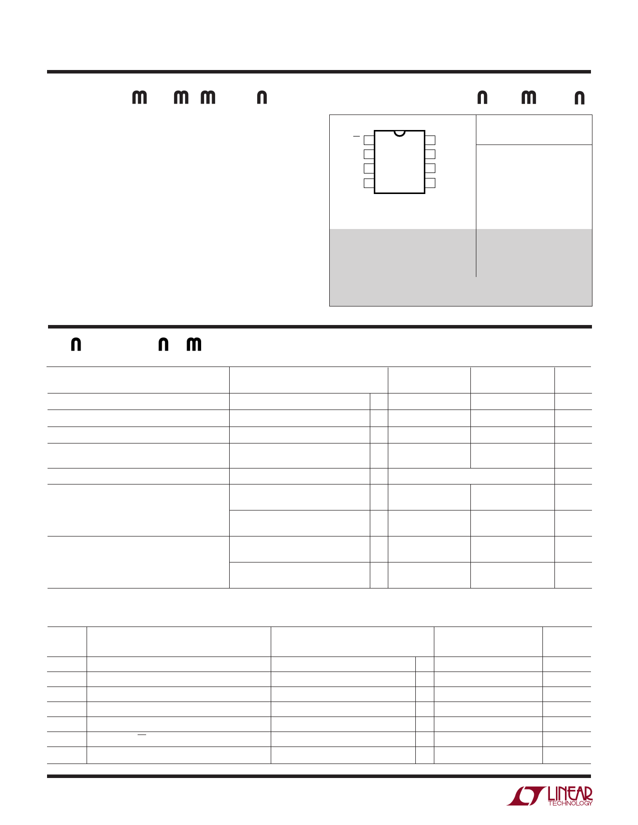
PACKAGE/ORDER I FOR ATIO
TOP VIEW
CS 1
+IN 2
8 VCC
7 CLK
–IN 3
GND 4
6 DOUT
5 VREF
N8 PACKAGE
8-LEAD PLASTIC DIP
TJMAX = 100°C, θJA = 130°C/W (N)
ORDER PART
NUMBER
LTC1287BCN8
LTC1287CCN8
J8 PACKAGE
8-LEAD CERAMIC DIP
TJMAX = 150°C, θJA = 100°C/W (J)
LTC1287BCJ8
LTC1287CCJ8
OBSOLETE PACKAGE
Consider N8 Package for Alternate Source
Consult LTC Marketing for parts specified with wider operating temperature ranges.
U
UW
CO VERTER A D ULTIPLEXER CHARACTERISTICS The q denotes the specifications
which apply over the full operating temperature range, otherwise specifications are at TA = 25°C. (Note 3)
PARAMETER
CONDITIONS
LTC1287B
LTC1287C
MIN TYP MAX MIN TYP MAX
UNITS
Offset Error
Linearity Error (INL)
Gain Error
VCC = 2.7V (Note 4)
q
±3.0
±3.0
LSB
VCC = 2.7V (Notes 4 & 5)
q
±0.5
± 0.5
LSB
VCC = 2.7V (Note 4)
q
±0.5
±1.0
LSB
Minimum Resolution for Which No
Missing Codes are Guaranteed
q
12
12
Bits
Analog and REF Input Range
(Note 7)
– 0.05V to VCC + 0.05V
V
On Channel Leakage Current (Note 8)
On Channel = 3V
Off Channel = 0V
q
±1
±1
µA
On Channel = 0V
Off Channel = 3V
q
±1
±1
µA
Off Channel Leakage Current (Note 8)
On Channel = 3V
Off Channel = 0V
q
±1
±1
µA
On Channel = 0V
Off Channel = 3V
q
±1
±1
µA
AC CHARACTERISTICS The q denotes the specifications which apply over the full operating temperature range,
otherwise specifications are at TA = 25°C. (Note 3)
LTC1287B/LTC1287C
SYMBOL PARAMETER
CONDITIONS
MIN TYP MAX
UNITS
fCLK
tSMPL
tCONV
tCYC
tdDO
tdis
ten
Clock Frequency
Analog Input Sample Time
Conversion Time
Total Cycle Time
Delay Time, CLK↓ to DOUT Data Valid
Delay Time, CS↑ to DOUT Hi-Z
Delay Time, CLK↓ to DOUT Enabled
(Note 6)
See Operating Sequence
See Operating Sequence
See Operating Sequence (Note 6)
See Test Circuits
See Test Circuits
See Test Circuits
(Note 9)
0.5
1.5
12
14 CLK+5.0µs
q
250 450
q
80 160
q
130 250
MHz
CLK Cycles
CLK Cycles
Cycles
ns
ns
ns
1287fa
2
Share Link: 