LTC1287CCN8 Просмотр технического описания (PDF) - Linear Technology
Номер в каталоге
Компоненты Описание
Список матч
LTC1287CCN8 Datasheet PDF : 16 Pages
| |||
APPLICATI S I FOR ATIO
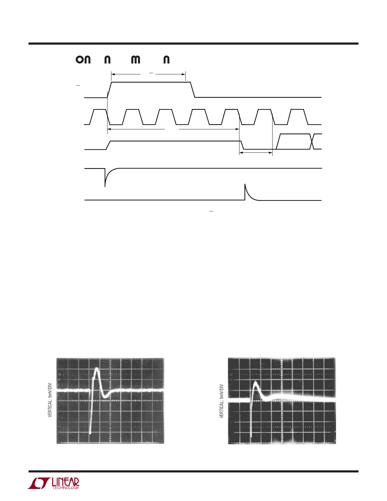
tWHCS
CS
LTC1287
CLK
DOUT
(+) INPUT
tSMPL
(+) INPUT MUST SETTLE DURING THIS TIME
HI-Z
B11
B10
1ST BIT TEST (–) INPUT MUST
SETTLE DURING THIS TIME
(–) INPUT
Figure 8c. Setup Time (tSUCS) is Not Met
LTC1287 F8c
effectively “held” by the sample and hold and will not affect
the conversion result. It is critical that the “–” input voltage
be free of noise and settle completely during the first CLK
cycle of the conversion. Minimizing RSOURCE– and C2 will
improve settling time. If large “–” input source resistance
must be used the time can be extended by using a slower
CLK frequency. At the maximum CLK frequency of 500kHz,
RSOURCE– < 200Ω and C2 < 20pF will provide adequate
settling.
Input Op Amps
When driving the analog inputs with an op amp it is
important that the op amp settles within the allowed time
(see Figures 8a, 8b and 8c). Again the “+” and “–” input
sampling times can be extended as described above to
accommodate slower op amps. For single supply low
voltage application the LT1797 and LT1677 can be made
to settle well even with the minimum settling windows of
6µs (“+” input) and 2µs (“–” input) which occur at the
maximum clock rates (CLK = 500kHz). Figures 9 and 10
show examples of adequate and poor op amp settling. The
LT1077, LT1078 or LT1079 can be used here to reduce
power consumption. Placing an RC network at the output
of the op amps will inprove the settling response and also
reduce the broadband noise.
HORIZONTAL: 500ns/DIV
Figure 9. Adequate Settling of Op Amp Driving Analog Input
HORIZONTAL: 20µs/DIV
Figure 10. Poor Op Amp Settling Can Cause A/D Errors
1287fa
11
Share Link: 