WSF2816-39H1MA Просмотр технического описания (PDF) - White Electronic Designs => Micro Semi
Номер в каталоге
Компоненты Описание
Список матч
WSF2816-39H1MA Datasheet PDF : 15 Pages
| |||
WSF2816-39XX
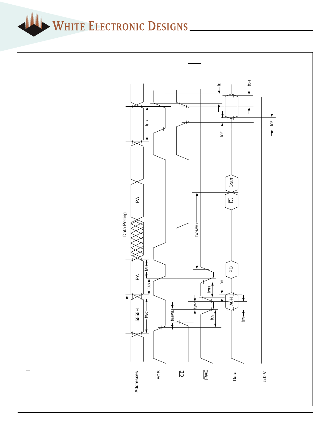
FIG. 8
WRITE/ERASE/PROGRAM OPERATION, FLASH MEMORY FWE CONTROLLED
NOTES:
1. PA is the address of the memory location to be
programmed.
2. PD is the data to be programmed at byte address.
3. D7 is the output of the complement of the data
written to the device.
4. DOUT is the output of the data written to
the device.
5. Figure indicates last two bus cycles of four bus
cycle sequence.
9
White Electronic Designs Corporation • (602) 437-1520 • www.whiteedc.com
Share Link: 