IDT74FCT3907SO Просмотр технического описания (PDF) - Integrated Device Technology
Номер в каталоге
Компоненты Описание
Список матч
IDT74FCT3907SO Datasheet PDF : 7 Pages
| |||
IDT74FCT3907
3.3V PC CLOCK SYNTHESIZER
COMMERCIAL TEMPERATURE RANGES
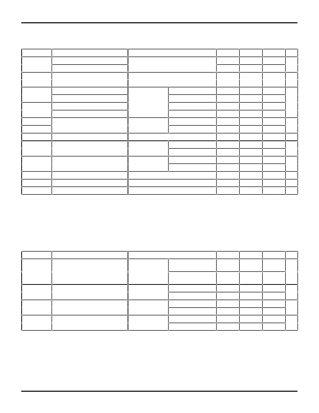
DC ELECTRICAL CHARACTERISTICS OVER OPERATING RANGE
Following Conditions Apply Unless Otherwise Specified:
Commercial: TA = 0°C to 70°C, VCC = 3.3V ± 0.3V
Symbol
VIH
Parameter
Input HIGH Level (Input pins)
Test Conditions(1)
Guaranteed Logic HIGH Level
Min.
2.0
Typ.(2)
—
Max. Unit
5.5
V
Input HIGH Level (I/O pins)
2.0
—
VCC+0.5
VIL
Input LOW Level
Guaranteed Logic LOW Level
–0.5
—
0.8
V
(Input and I/O pins)
II H
Input HIGH Current (Input pins)(5) VCC = Max.
VI = 5.5V
—
—
±1
µA
Input HIGH Current (I/O pins)(5)
II L
Input LOW Current (Input pins)(5)
Input LOW Current (I/O pins)(5)
VI = VCC
VI = GND
VI = GND
—
—
±1
—
—
±1
—
—
±1
IOZH
IOZL
High Impedance Output Current
(3-State Output pins)((6)
VCC = Max.
VO = VCC
VO = GND
—
—
±1
µA
—
—
±1
VIK
Clamp Diode Voltage
VCC = Min., IIN = –18mA
—
–0.7
–1.2 V
VOH
Output HIGH Voltage
VCC = Min.
IOH = –0.1mA
VCC–0.2
—
—
V
VIN = VIH or VIL IOH = –8mA COM'L. VCC–0.6V 3.0
—
VOL
Output LOW Voltage
VCC = Min.
IOL = 0.1mA
—
—
0.2
V
VIN = VIH or VIL IOL = 8mA
—
0.3
0.5
IOS
Short Circuit Current(4,6)
VCC = Max., VO = GND(3)
–43
–135
–206 mA
IOS
Short Circuit Current(4,7)
VCC = Max., VO = GND(3)
–34
–135
–195 mA
ICCZ
Quiescent Power Supply Current VCC = Max., VIN = GND or VCC
—
3.0
4.0 mA
NOTES:
1. For conditions shown as Max. or Min., use appropriate value specified under Electrical Characteristics for the applicable device type.
2. Typical values are at Vcc = 3.3V, +25°C ambient.
3. Not more than one output should be tested at one time. Duration of the test should not exceed one second.
4. This parameter is guaranteed but not tested.
5. The test limit for this parameter is ±5µA at TA = –55°C.
6. Applies to CPUCLK.
7. Applies to PCICLK.
3245 tbl 05
DYNAMIC OUTPUT DRIVE CHARACTERISTICS
Symbol
IODH
Parameter
CPUCLK Output HIGH Current
IODH
PCICLK Output HIGH Current
Test Conditions(1)
VIN = VIH or VIL, VCC = 3.135V
(3.3V –5%)
VOUT = 2.4V
VCC = 3.465V
(3.3V +5%)
VIN = VIH or VIL, VCC = 3.135V
Min.
–23
—
–14.5
Typ.(2)
Max. Unit
—
mA
–109
—
mA
VOUT = 2.4V
VCC = 3.465V
—
–100
IODL
CPUCLK Output LOW Current
VIN = VIH or VIL, VCC = 3.135V
16
—
mA
VOUT = 0.4V
VCC = 3.465V
—
40
IODL
PCICLK Output LOW Current
VIN = VIH or VIL, VCC = 3.135V
9.4
—
mA
VOUT = 0.4V
VCC = 3.465V
—
38
NOTES:
1. For conditions shown as Max. or Min., use appropriate value specified under Electrical Characteristics for the applicable device type.
2. Typical values are at Vcc = 3.3V, +25°C ambient.
3. Not more than one output should be tested at one time. Duration of the test should not exceed one second.
4. This parameter is guaranteed but not tested.
5. The test limit for this parameter is ±5µA at TA = –55°C.
3245 tbl 06
9.10
3
Share Link: 