MB40950PF Просмотр технического описания (PDF) - Fujitsu
Номер в каталоге
Компоненты Описание
Список матч
MB40950PF Datasheet PDF : 11 Pages
| |||
MB40950
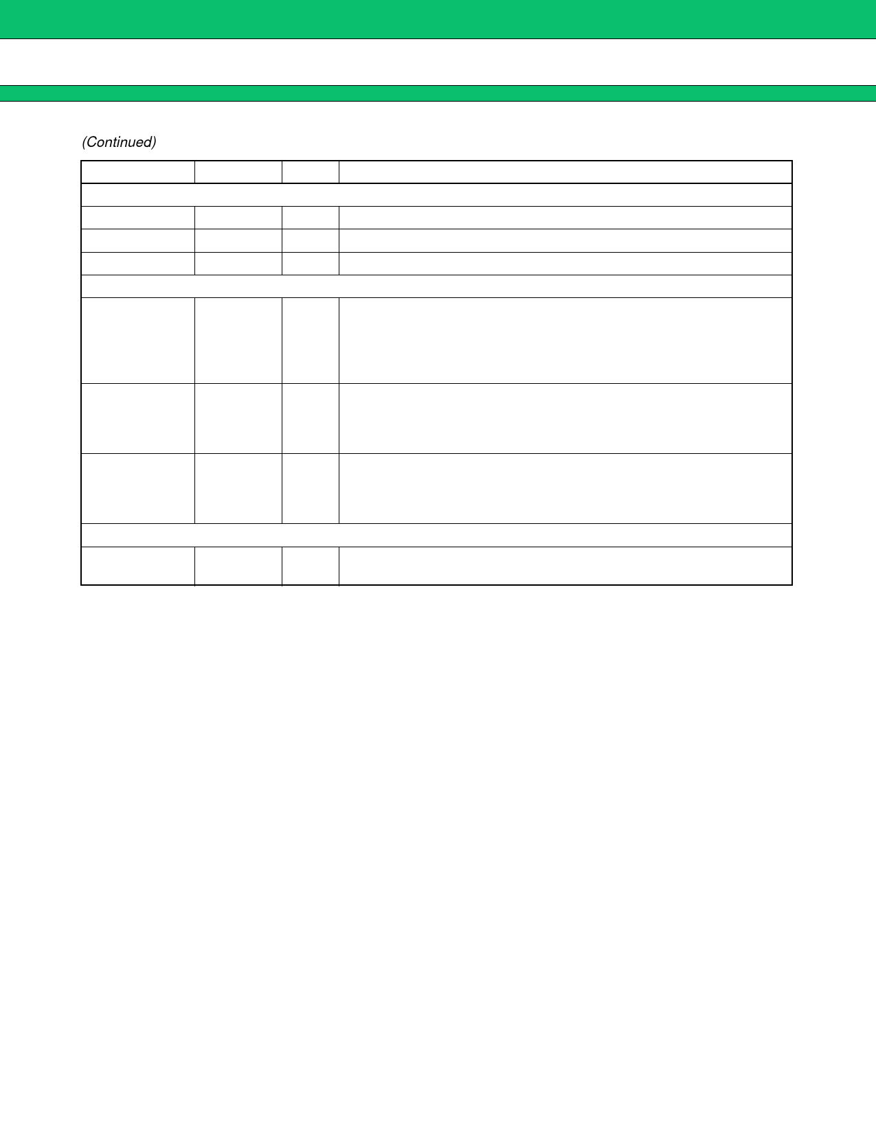
(Continued)
Symbol
Pin No.
Analog Output
ROUT
46
GOUT
43
BOUT
40
Reference Voltage
VRIN
37
VROUT1
36
VROUT2
38
Compesation Capacitor
COMP
35
Type
Name & Function
O Analog signal output pin for R channel.
O Analog signal output pin for G channel.
O Analog signal output pin for B channel.
Reference voltage input pin. This pin is used to set the analog output
dynamic range. When the internal reference voltage is used, this pin is
I connected with VROUT1 pin (36 pin) or VROUT2 pin (38 pin). When the
reference voltage is supplied from the external generator, 2.65V to
4.3V or VCCA - VRIN = 0.7V to 2.2V is input to this pin.
Reference voltage output #1 pin. The output voltage is set to 0.6 x
O
VCCA by the resistor divided method. When this pin is connected with
VRIN pin (37 pin), an analog voltage is output from this pin in a range of
0.6 x VCCA to VCCA.
Reference voltage output #2 pin. The output voltage is set to VCCA - 2V
O
by the band-gap reference method. When this pin is connected with
VRIN pin (37 pin), an analog voltage is output from this pin in a range of
VCCA - 2V to VCCA.
-
Phase compesation capacitor pin. A phase compesation capacitor of
0.1µF or greater is connected between this pin and A. GND pin.
4
Share Link: 