AS1326 Просмотр технического описания (PDF) - austriamicrosystems AG
Номер в каталоге
Компоненты Описание
Список матч
AS1326 Datasheet PDF : 18 Pages
| |||
AS1326
Datasheet - Detailed Description
8 Detailed Description
The AS1326A/AS1326B are high-efficiency, low-noise DC-DC boost converters suitable as power supplies for portable
devices. Both devices feature integrated boost switching regulator, N-channel power MOSFET, P-channel synchro-
nous rectifier, precision reference, and shutdown control circuitry (see Figure 1 on page 1).
The AS1326A/AS1326B are able to boost a 1- to 3-cell battery voltage input to a fixed 3.3V output, or adjustable output
between 2.5 and 5.0V (an external Schottky diode is required for output voltages greater than 4V).
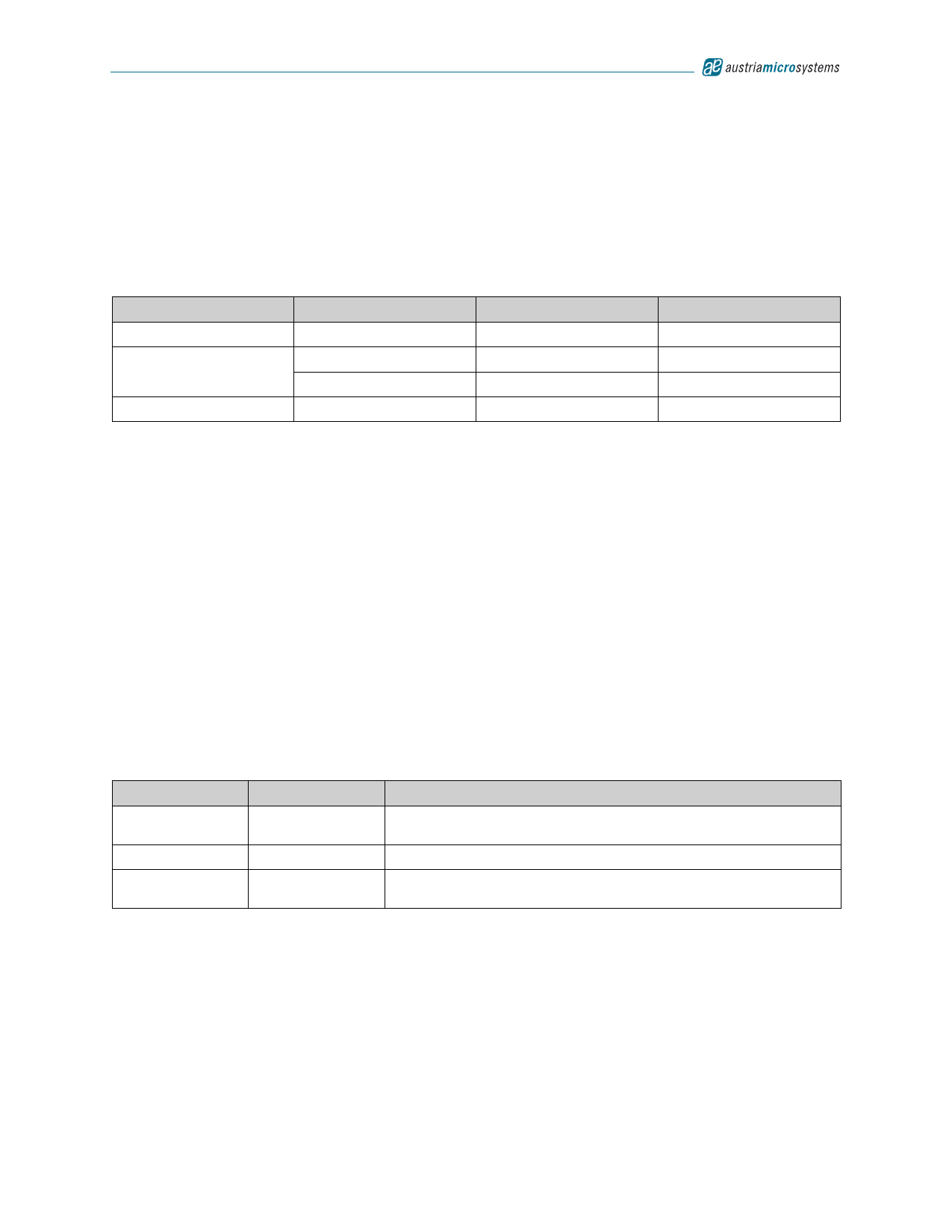
Table 5. Typical Output Voltages and Currents
# of NiCd/NiMh Cells
Input Voltage (V)
Output Voltage (V)
Output Current (mA)
1
1.2
3.3
335
2.4
3.3
800
2
2.4
5.0
450
3
3.6
5.0
800
The devices are guaranteed to startup with an input voltage as low as 1.1V and remain operational down to an input of
as little as 0.7V, and are optimized for use in mobile phones and other RF applications which have low noise and low
quiescent current (extended battery life) requirements.
The integrated shutdown circuitry reduces device quiescent current down to 0.1µA.
Step-Up Converter
During boost operation, the internal N-channel MOSFET switch turns on for the first part of each cycle, allowing current
to ramp up in the inductor and store energy in a magnetic field. During the second part of each cycle, the MOSFET
turns off and inductor current flows through the synchronous rectifier to the output filter capacitor and the load. As the
energy stored in the inductor is depleted, the current ramps down and the synchronous rectifier turns off.
At light loads, the device operates at fixed-frequency or only as needed to maintain regulation, depending on the set-
ting of pin CLK/SEL (see Table 6).
Operational Modes
The AS1326A/AS1326B are capable of operating in 3 different modes (see Table 6) as controlled by pin CLK/SEL (see
page 2).
Table 6. Operational Modes
CLK/SEL Setting Operational Mode
0
Normal
1
Forced PWM
External 500kHz to
1.2MHz clock
Synchronized PWM
Description
High-efficiency at all loads; Fixed-frequency (1MHz) at heavy and
medium loads.
Fixed-frequency (1MHz), low-noise at all loads. VIN ≤ 0.75xVOUT
Fixed-frequency, low-noise at all loads. VIN ≤ 0.75xVOUT
Normal Operation
When CLK/SEL is pulled low, the devices are in normal operating mode. In normal mode the devices operate in PWM
when driving medium-to-heavy loads, and automatically switches to automatic powersave mode if the load requires
less power. The use of automatic powersave mode will boost the efficiency futhermore at light-load conditions.
Forced-PWM Operation
Pulling CLK/SEL high, selects the low-noise PWM-only mode. During forced-PWM operation, the devices switch at a
constant frequency (1MHz) and modulates the MOSFET switch pulse width to control the power transferred per cycle
to regulate the output voltage. Switching harmonics generated by fixed-frequency operation are consistent and can be
filtered. See the Noise Spectrum plot in the Typical Operating Characteristics (see Figure 14 on page 7).
www.austriamicrosystems.com
Revision 1.05
9 - 18
Share Link: 