AS1326 Просмотр технического описания (PDF) - austriamicrosystems AG
Номер в каталоге
Компоненты Описание
Список матч
AS1326 Datasheet PDF : 18 Pages
| |||
AS1326
Datasheet - Application Information
9 Application Information
Figure 19. Typical AS1326A Application Circuit
VIN = 2.4V
+
33µF
3.3µH
10nF
8
LX
10
ONN
6
CLK/SEL
1
ISET
2
REF
4
FB
3
GND
7
PGND
AS1326A
9
POUT
10Ω
+
100µF
5
OUT
330nF
VOUT = 3.3V
800mA
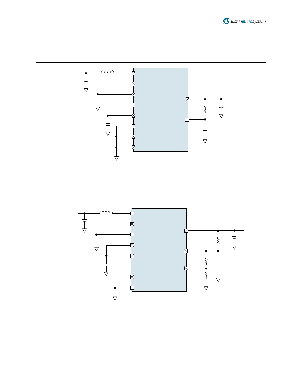
Setting the Output Voltages
For a fixed 3.3V output, connect pin FB to GND. To set adjustable output voltages between 2.5 and 5.0V, connect a
resistor voltage-divider to pin FB from pin OUT to GND (Figure 20).
Figure 20. Application Circuit using External Feedback Resistors
VIN = 2.4V
+
33µF
3.3µH
10nF
8
LX
10
ONN
6
CLK/SEL
1
ISET
2
REF
AS1326A
3
GND
7
PGND
9
POUT
5
OUT
R1
4
FB
R2
+
100µF
10Ω
330nF
VOUT
For the circuit shown in Figure 20, the input bias current into FB is <20nA, permitting large-value resistor-divider net-
works while maintaining accuracy. Place the resistor-divider network as close to the device as possible. Use a ≤ 270kΩ
resistor for R2, then calculate R1 as:
R1
=
R2
⋅
⎛
⎝
V-----O----U----T-
VFB
–
1⎠⎞
(EQ 1)
Where:
VFB (the boost-regulator feedback set point) is 1.24V.
www.austriamicrosystems.com
Revision 1.05
11 - 18
Share Link: 