ADM488ABRZ Просмотр технического описания (PDF) - Analog Devices
Номер в каталоге
Компоненты Описание
Список матч
ADM488ABRZ Datasheet PDF : 16 Pages
| |||
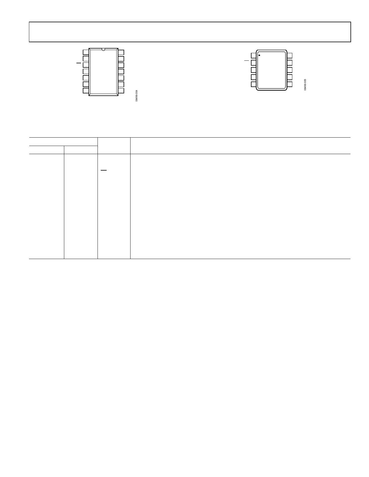
NC 1
RO 2
RE 3
DE 4
DI 5
GND 6
GND 7
ADM489A
TOP VIEW
(Not to Scale)
14 VCC
13 NC
12 A
11 B
10 Z
9Y
8 NC
NC = NO CONNECT
Figure 4. ADM489A SOIC_N Pin Configuration
ADM488A/ADM489A
RO 1
RE 2
DE 3
DI 4
GND 5
ADM489A
TOP VIEW
(Not to Scale)
10 VCC
9A
8B
7Z
6Y
Figure 5. ADM489A MSOP Pin Configuration
Table 5. ADM489A Pin Function Descriptions
Pin No.
SOIC_N
MSOP
Mnemonic Description
1, 8, 13
N/A1
NC
No Connect. No connections are required to this pin.
2
1
RO
Receiver Output. When enabled, if A > B by 200 mV, RO = high. If A < B by 200 mV, RO = low.
3
2
RE
Receiver Output Enable. A low level enables the receiver output, RO. A high level places the
ADM489A in a high impedance state.
4
3
DE
Driver Output Enable. A high level enables the driver differential outputs (Y and Z). A low level
places the ADM489A in a high impedance state.
5
4
DI
Driver Input. When the driver is enabled, a logic low on DI forces Y low and Z high, whereas a
logic high on DI forces Y high and Z low.
6, 7
5
GND
Ground Connection, 0 V.
9
6
Y
Noninverting Driver, Differential Output Y.
10
7
Z
Inverting Driver, Differential Output Z.
11
8
B
Inverting Receiver, Input B.
12
9
A
Noninverting Receiver, Input A.
14
10
VCC
Power Supply, 5 V ± 10%.
1 N/A means not applicable.
Rev. 0 | Page 7 of 16
Share Link: 