ADM488ABRZ Просмотр технического описания (PDF) - Analog Devices
Номер в каталоге
Компоненты Описание
Список матч
ADM488ABRZ Datasheet PDF : 16 Pages
| |||
ADM488A/ADM489A
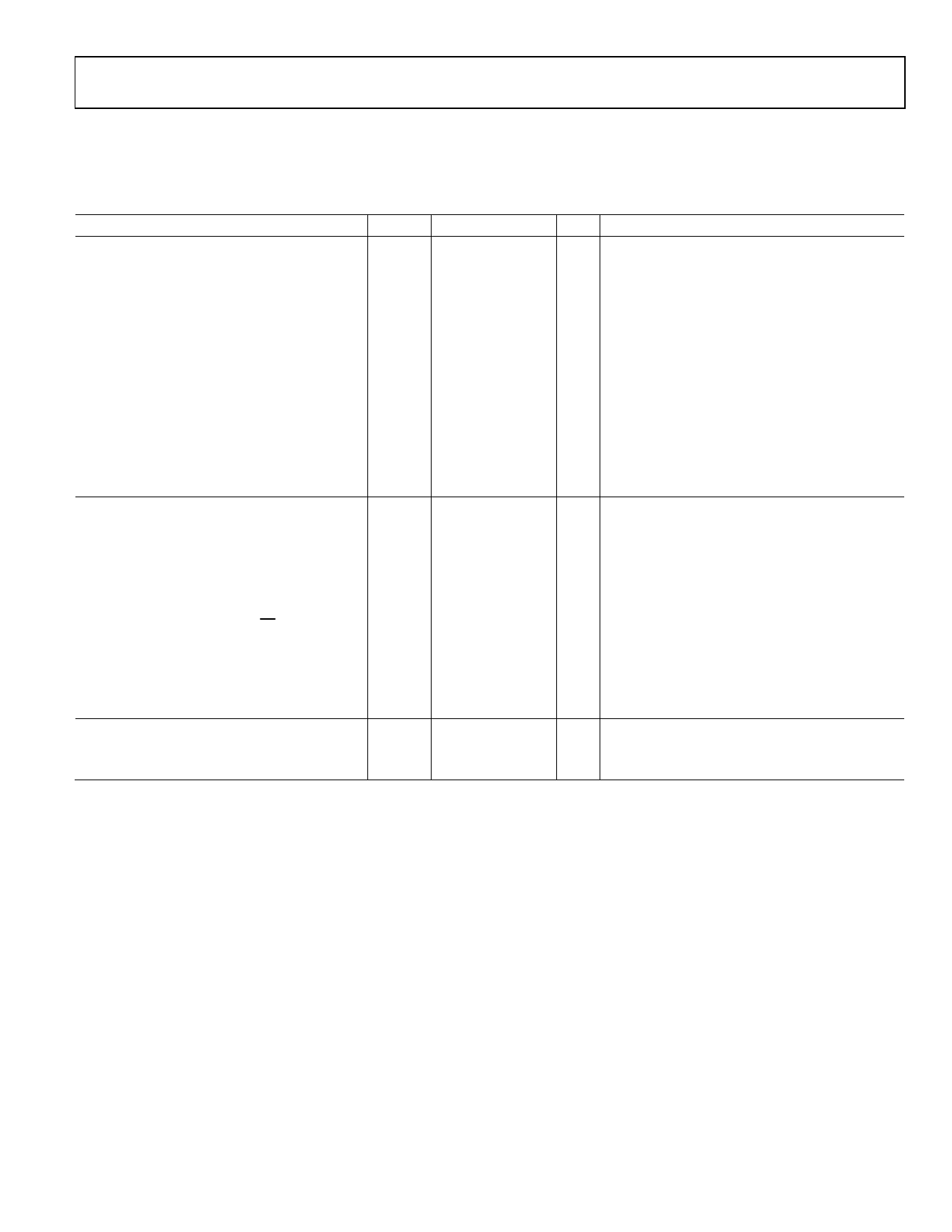
SPECIFICATIONS
VCC = 5 V ± 10%; all specifications TMIN to TMAX, unless otherwise noted.
Table 1.
Parameter
DRIVER
Differential Output Voltage
Δ|VOD| for Complementary Output States
Common-Mode Output Voltage
Δ|VOC| for Complementary Output States
Output Short-Circuit Current
VOUT
CMOS Input Logic Threshold Low
CMOS Input Logic Threshold High
Logic Input Current (DE, DI)
RECEIVER
Differential Input Threshold Voltage
Input Voltage Hysteresis
Input Resistance
Input Current (A, B)
Logic Enable Input Current (RE)
CMOS Output Voltage Low
CMOS Output Voltage High
Short-Circuit Output Current
Three-State Output Leakage Current
POWER SUPPLY CURRENT
Symbol Min Typ Max Unit Test Conditions/Comments
VOD
2.0
1.5
1.5
VOC
5.0 V
5.0 V
5.0 V
5.0 V
0.2 V
3.0 V
0.2 V
R = ∞, see Figure 11
VCC = 5 V, R = 50 Ω (RS-422), see Figure 11
R = 27 Ω (RS-485), see Figure 11
VTST = –7 V to +12 V, see Figure 12, VCC = 5 V ± 5%
R = 27 Ω or 50 Ω, see Figure 11
R = 27 Ω or 50 Ω, see Figure 11
R = 27 Ω or 50 Ω
250 mA −7 V ≤ VO ≤ +12 V
VINL
1.4 0.8 V
VINH
2.0 1.4
V
±1.0 μA
VTH
ΔVTH
VOL
VOH
ICC
−0.2
70
12
4.0
7
30
37
+0.2 V
mV
kΩ
1 mA
−0.8 mA
±1 μA
0.4 V
V
85 mA
±1.0 μA
60 μA
74 μA
−7 V ≤ VCM ≤ +12 V
VCM = 0 V
−7 V ≤ VCM ≤ +12 V
VIN = 12 V
VIN = −7 V
IOUT = +4.0 mA
IOUT = −4.0 mA
VOUT = GND or VCC
0.4 V ≤ VOUT ≤ 2.4 V
Outputs unloaded, receivers enabled
DE = 0 V (disabled)
DE = 5 V (enabled)
Rev. 0 | Page 3 of 16
Share Link: 