ADM2483BRW Просмотр технического описания (PDF) - Analog Devices
Номер в каталоге
Компоненты Описание
Список матч
ADM2483BRW Datasheet PDF : 20 Pages
| |||
ADM2483
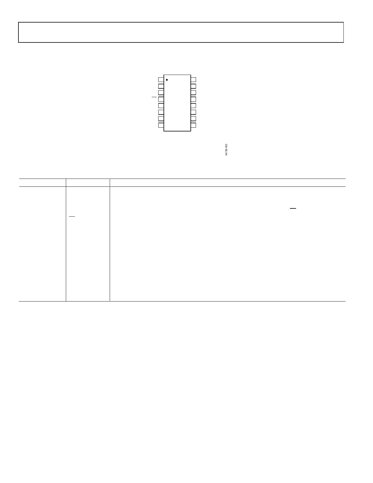
PIN CONFIGURATION AND FUNCTION DESCRIPTIONS
Data Sheet
VDD1 1
16 VDD2
GND11 2
15 GND21
RxD 3 ADM2483 14 NC
RE 4 TOP VIEW 13 B
DE 5 (Not to Scale) 12 A
TxD 6
11 NC
PV 7
10 NC
GND11 8
9 GND21
NC = NO CONNECT
1 PIN 2 AND PIN 8 ARE INTERNALLY CONNECTED.
EITHER OR BOTH MAY BE USED FOR GND1.
PIN 9 AND PIN 15 ARE INTERNALLY CONNECTED.
EITHER OR BOTH MAY BE USED FOR GND2.
Table 8. Pin Function Descriptions
Pin No.
Mnemonic
1
VDD1
2, 8
GND1
3
RxD
4
RE
5
6
7
9, 15
10, 11, 14
12
DE
TxD
PV
GND2
NC
A
13
B
16
VDD2
Figure 2. Pin Configuration
Description
Power Supply (Logic Side).
Ground (Logic Side).
Receiver Output Data. When enabled, if (A − B) ≥ −30 mV, then RxD = high. If (A − B) ≤ −200 mV, then
RxD = low. This is a tristate output when the receiver is disabled, that is, when RE is driven high.
Receiver Enable Input. This is an active-low input. Driving this input low enables the receiver, and
driving it high disables the receiver.
Driver Enable Input. Driving the input high enables the driver, and driving it low disables the driver.
Transmit Data Input. Data to be transmitted by the driver is applied to this input.
Power_Valid. Used during power-up and power-down. See the Applications Information section.
Ground (Bus Side).
No Connect.
Noninverting Driver Output/Receiver Input. When the driver is disabled, or when VDD1 or VDD2 is
powered down, Pin A is put into a high impedance state to avoid overloading the bus.
Inverting Driver Output/Receiver Input. When the driver is disabled, or when VDD1 or VDD2 is powered
down, Pin B is put into a high impedance state to avoid overloading the bus.
Power Supply (Bus Side).
Rev. C | Page 8 of 20
Share Link: 